
 My Inquiry
 My Account


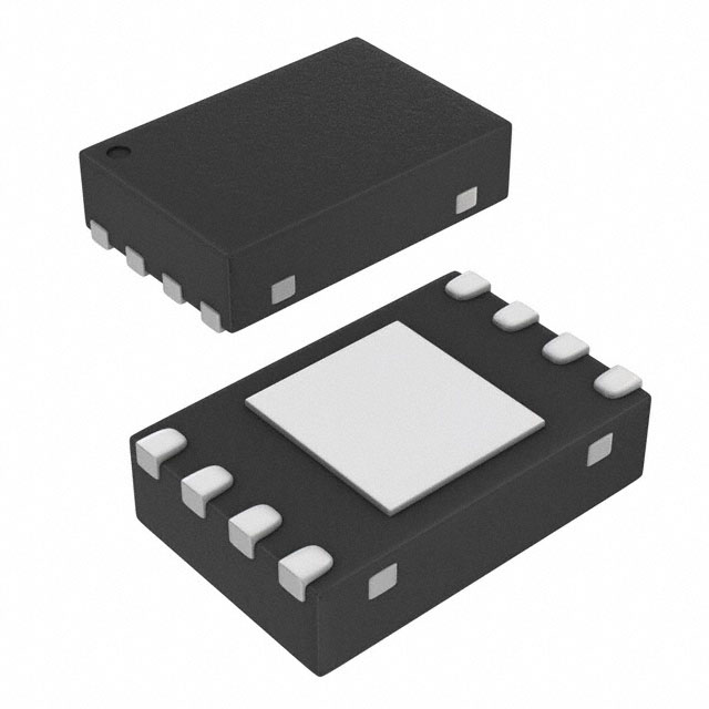
Renesas TSE2002B3CNCG8
- Part No.:
- TSE2002B3CNCG8
- Manufacturer:
- Renesas
- Category:
- Thermal Management
- Package:
- 8-WFDFN Exposed Pad
- Datasheet:
-
 TSE2002B3CNCG8.pdf
- Description:
- IC TEMP SENS EEPROM TDFN-8
- Quantity:
- Payment:

- Shipping:

Inventory:3,046
Please send an inquiry. Send us your inquiry, and we will respond immediately.
Product details
Overview
TSE2002B3CNCG8 from Integrated Device Technology (IDT) is a JEDEC JC42.4-compliant digital temperature sensor with integrated 256-byte serial EEPROM, designed for DDR2/DDR3 DIMM modules. It delivers ±0.5°C accuracy from –20°C to +125°C, supports programmable resolution down to 0.0625°C, and features an open-drain EVENT pin for memory throttling in server and laptop memory subsystems.
For engineers reviewing the TSE2002B3CNCG8 datasheet, TSE2002B3CNCG8 pinout, TSE2002B3CNCG8 application, or TSE2002B3CNCG8 equivalent, key selection criteria include SMBus timeout compliance (25–35 ms), dual-function I²C interface (temperature + SPD EEPROM), SA0–SA2 address configuration, and write-protection modes for SPD sector locking.
Technical Context
The TSE2002B3CNCG8 integrates two independent functional blocks on a single die: a high-accuracy sigma-delta ADC-based temperature sensor with configurable hysteresis (0/1.5/3/6°C) and resolution (9–12 bit), and a 2Kbit (256×8) EEPROM organized as one block with software write protection (SWP/CWP/PSWP). Both blocks share a common 2-wire I²C/SMBus interface operating at 10–400 kHz.
It implements three distinct EVENT pin modes - Interrupt, Comparator, and Critical-Only - each governed by register-controlled polarity and status-clearing logic. The device uses separate Device Type Identifier Codes (0011b for TS registers, 1010b for SPD memory, 0110b for write-protection commands) to multiplex functions over the same bus without external logic.
Key Specifications
| Parameter | Value and Actual Design Meaning |
|---|---|
| Temp Accuracy | ±0.5°C (typ.) from –20°C to +125°C - meets JEDEC B-grade for DIMM thermal monitoring |
| Resolution | 0.0625°C (12-bit) to 0.5°C (9-bit) - selectable via config register for trade-off between precision and conversion time |
| EEPROM Size | 256 bytes (2Kbit), organized as single block - supports full SPD data storage per JEDEC specification |
| Supply Voltage | 3.0 V to 3.6 V - compatible with DDR2/DDR3 module VDDSPD rails |
| SMBus Timeout | 25 ms (min) / 35 ms (max) - ensures robust bus recovery in multi-device memory systems |
| Sampling Rate | ≤100 ms per conversion - enables real-time thermal event detection for memory throttling |
| Hysteresis | Selectable 0, 1.5°C, 3°C, or 6°C - prevents chattering during temperature threshold crossings |
Pinout & Package
Package: DFN-8 (3 mm × 3 mm, 0.5 mm pitch), RoHS-compliant, moisture sensitivity level 1.
| Pin/Terminal | Circuit Role | Design Meaning |
|---|---|---|
| 1 (SA0) | Slave Address Input / VHV Detection | Configures LSB of 7-bit I²C address; also detects high-voltage (≥4.8 V) for SWP/PSWP command decoding |
| 2 (SA1) | Slave Address Input | Configures middle bit of 7-bit I²C address; must be hard-wired to VDDSPD or VSSSPD |
| 3 (SA2) | Slave Address Input | Configures MSB of 7-bit I²C address; enables up to eight devices on same SMBus |
| 4 (VSSSPD) | Ground Reference | Dedicated ground pin for SPD/TS circuitry - decouples noise from shared VDDSPD rail |
| 5 (SDA) | I²C Bidirectional Data Line | Open-drain output with Schmitt trigger input - supports wire-OR topology and noise filtering |
| 6 (SCL) | I²C Clock Input | Input-only clock line with internal noise filter - tolerates glitches <50 ns above 100 kHz |
| 7 (EVENT) | Open-Drain Event Output | Asserts on temp limit violation; polarity and mode (Interrupt/Comparator/TCRIT-only) are software-configurable |
| 8 (VDDSPD) | Power Supply | 3.0–3.6 V supply for both temperature sensor and EEPROM - no separate analog/digital rails required |
Key Features
| Feature | Design Value |
|---|---|
| JEDEC JC42.4 Compliance | Fully compliant with industry-standard memory module thermal monitoring spec - ensures interoperability with MCH and memory controllers |
| Permanent SPD Write Protection | PSWP command locks addresses 0x00–0x7F permanently - prevents accidental overwrite of critical DRAM configuration data |
| Configurable EVENT Polarity | Active-high or active-low output via register setting - eliminates need for external inverters in host controller interfaces |
| Timeout-Safe SMBus Interface | Guaranteed 25–35 ms clock low timeout - enables reliable bus arbitration and recovery in dense DIMM configurations |
| Independent Power Modes | Temperature sensor can be shut down while EEPROM remains active (or vice versa) - reduces system power during idle periods |
Applications
| DDR2/DDR3 DIMM Thermal Monitoring | Server Memory Subsystem Throttling |
|---|---|
Use Scenario: Real-time temperature tracking of dual-inline memory modules during high-bandwidth operation in desktop and workstation platforms. IC Role / Device Role / Timing Role: Primary JEDEC-compliant temperature sensor and SPD EEPROM for DDR2/DDR3 modules - provides thermal data and module configuration to memory controller. Use Value: Enables dynamic memory frequency scaling when temperature exceeds TCRIT, preventing thermal damage while maintaining JEDEC SPD compatibility. | Use Scenario: Coordinated thermal management across multiple DIMMs in 1U/2U rack-mounted servers with high-density memory layouts. IC Role / Device Role / Timing Role: Distributed temperature node feeding EVENT signals to baseboard management controller (BMC) for cross-DIMM throttling decisions. Use Value: Delivers sub-1°C accuracy and deterministic 100 ms sampling - allows precise, low-latency intervention before thermal runaway occurs. |
| Laptop/Ultrabook Memory Management | Industrial Memory Module Calibration |
Use Scenario: Compact memory modules in fanless or thermally constrained ultraportable designs requiring minimal footprint and low quiescent current. IC Role / Device Role / Timing Role: Dual-function sensor+EEPROM in space-constrained SO-DIMM form factor - replaces discrete SPD EEPROM and external temp sensor. Use Value: Reduces BOM count by two components and eliminates routing complexity for separate SDA/SCL and TEMP lines. | Use Scenario: High-reliability memory modules used in industrial control systems where SPD data integrity must survive extended temperature cycling and field updates. IC Role / Device Role / Timing Role: Secure SPD storage with permanent write protection (PSWP) and verified JEDEC read/write timing - ensures configuration persistence over 10+ years. Use Value: Prevents field corruption of access speed, density, and timing parameters - critical for deterministic boot and runtime memory initialization. |
Equivalent & Alternatives
The following parts are listed as comparable options for similar temperature-sensing-with-SPD-EEPROM applications.
| Alternative Part | Technical Difference | Application Difference | Selection Advice |
|---|---|---|---|
| AT30TS74-MA8Y | ±0.5°C accuracy, 128-byte EEPROM, no PSWP support, 1.7–5.5 V supply | Lacks permanent SPD lock; wider voltage range but not JEDEC JC42.4 certified | Use where JEDEC compliance is not mandatory and lower EEPROM capacity suffices |
| NCP1022DR2G | ±1.0°C accuracy, no EEPROM, 2.7–5.5 V, 6-pin SOT-23 | Discrete temperature sensor only - requires external SPD EEPROM and address logic | Choose only if system already implements separate SPD memory and needs lowest-cost thermal sensing |
Compared with AT30TS74-MA8Y and NCP1022DR2G, the TSE2002B3CNCG8 uniquely combines JEDEC JC42.4 certification, permanent SPD write protection, and dual-mode EVENT signaling - making it the only drop-in solution for DDR2/DDR3 DIMM manufacturers requiring full specification compliance and field-programmable thermal policy enforcement.
Availability
TSE2002B3CNCG8 is available at Aetrix Electronics and suitable for DDR2/DDR3 DIMM manufacturing, server memory subsystem design, and industrial memory module calibration requiring stable component supply, long-term lifecycle support, and JEDEC-compliant thermal monitoring.
Supply support for TSE2002B3CNCG8 includes scheduled delivery planning, volume procurement assistance, BOM continuity management, traceable sourcing, and lifecycle availability coordination for OEM customers, industrial embedded developers, connected-device designers, and electronics production programs.
Manufacturer
Integrated Device Technology (IDT) was a fabless semiconductor company specializing in timing, memory interface, RF, and sensor solutions before its acquisition by Renesas Electronics in 2019. IDT pioneered JEDEC-compliant memory interface ICs.
The TSE2002B3CNCG8 belongs to IDT's memory module sensor product line, engineered specifically to meet JEDEC JC42.4 requirements for DDR2/DDR3 SPD and thermal monitoring - targeting DIMM manufacturers needing integrated, certified, and production-ready solutions.
FAQ
What is the primary application of the TSE2002B3CNCG8?
The TSE2002B3CNCG8 is primarily used as a JEDEC JC42.4-compliant temperature sensor and SPD EEPROM for DDR2 and DDR3 memory modules. It provides accurate thermal monitoring and stores critical DRAM configuration data such as access speed, size, and organization. Its integrated EVENT pin enables direct memory throttling in laptops, servers, and workstations - making TSE2002B3CNCG8 essential for thermal-aware memory subsystems that require both precision sensing and secure SPD storage.
Does the TSE2002B3CNCG8 support permanent write protection of SPD data?
Yes, the TSE2002B3CNCG8 supports permanent write protection of the lower 128 bytes (0x00–0x7F) via the PSWP (Permanently Set Write Protection) command. Once executed, this protection cannot be cleared by software, power cycling, or hardware reset - ensuring SPD configuration data remains immutable in deployed DIMMs. This feature is explicitly defined in the TSE2002B3CNCG8 datasheet and is a key differentiator for high-reliability memory applications where field corruption must be prevented.
What are the supported I²C/SMBus speeds for the TSE2002B3CNCG8?
The TSE2002B3CNCG8 supports standard-mode and fast-mode I²C/SMBus operation from 10 kHz to 400 kHz. Its AC characteristics guarantee tTIMEOUT of 25–35 ms, meeting strict SMBus specification requirements. The device does not support high-speed mode (>400 kHz) or clock stretching. All timing parameters - including tSU:STA, tHD:DAT, and tW - are validated across the full 3.0–3.6 V supply range and –20°C to +125°C ambient temperature, ensuring robust interoperability in multi-drop memory bus environments.
How is the slave address configured on the TSE2002B3CNCG8?
The TSE2002B3CNCG8 uses three hardware address pins - SA0, SA1, and SA2 - to configure the three LSBs of its 7-bit I²C slave address. These pins must be hard-wired to either VDDSPD or VSSSPD (not pulled via resistors) to establish a unique address. Combined with a fixed 4-bit Device Type Identifier (0011b for temperature registers, 1010b for SPD memory), this allows up to eight TSE2002B3CNCG8 devices on a single bus. The full address is validated in the TSE2002B3CNCG8 datasheet's I²C Operating Modes table.
What is the function of the EVENT pin on the TSE2002B3CNCG8?
The EVENT pin on the TSE2002B3CNCG8 is an open-drain output that signals temperature threshold violations. It operates in three configurable modes: Interrupt (latched until cleared by register write), Comparator (self-clearing when condition resolves), or Critical-Only (asserts only on TCRIT exceedance). Polarity (active-high/low) and mode are set via internal registers. The pin requires an external pull-up to VDDSPD and is used directly by memory controllers for thermal throttling - a core function confirmed in the TSE2002B3CNCG8 block diagram and pin description sections.
TSE2002B3CNCG8 Specifications
- Product attributes
- Attribute value
- Manufacturer:
- Renesas
- Series:
- -
- Package/Case:
- 8-WFDFN Exposed Pad
- Packaging:
- Tape & Reel (TR)
- Product Status:
- Obsolete
- Function:
- Temp Monitoring System (Sensor)
- Sensor Type:
- Internal
- Sensing Temperature:
- -20°C ~ 125°C
- Accuracy:
- ±1°C(Max)
- Topology:
- ADC (Sigma Delta), Control Logic, Register Bank
- Output Type:
- 2-Wire Serial, I2C/SMBUS
- Output Alarm:
- No
- Output Fan:
- No
- Voltage - Supply:
- 3V ~ 3.6V
- Operating Temperature:
- -20°C ~ 125°C
- Grade:
- -
- Qualification:
- -
- Mounting Type:
- Surface Mount
- Supplier Device Package:
- 8-VFQFPN (2x3)
TSE2002B3CNCG8 FAQ
1.How can I place an order for TSE2002B3CNCG8 through Aetrix?
Please submit a Request for Quotation (RFQ) for TSE2002B3CNCG8 on Aetrix. Our sales agent will provide a competitive quotation and guide you through the order confirmation once you accept the terms.
2.Are the price and stock information for TSE2002B3CNCG8 reliable?
The price and inventory of TSE2002B3CNCG8 are updated periodically and may fluctuate due to market conditions. Stock and pricing data are typically refreshed every 24 hours. Quotation validity for TSE2002B3CNCG8 is usually 5 days.
3.What payment methods are accepted for TSE2002B3CNCG8?
We accept Wire Transfer, PayPal, Credit Card, Western Union, MoneyGram, and Escrow for TSE2002B3CNCG8 transactions.
Note: Certain payment methods may incur a processing fee.
4.How is shipping managed for TSE2002B3CNCG8?
TSE2002B3CNCG8 orders can be shipped via leading logistics carriers, including DHL, UPS, FedEx, TNT, or Registered Mail.
Once your TSE2002B3CNCG8 order is processed, you will receive an email with the shipment details and tracking number.
Note: Tracking information may take up to 24 hours to appear. Express delivery typically takes 3–5 business days.
5.How can I obtain technical support or documentation for TSE2002B3CNCG8?
For technical support, including TSE2002B3CNCG8 datasheets, pinout diagrams, or application guidance, please contact our engineering support team. They can provide detailed documentation and assistance for your TSE2002B3CNCG8 requirements.
6.How does Aetrix verify that TSE2002B3CNCG8 is sourced from the original manufacturer or authorized distributors?
All TSE2002B3CNCG8 products on Aetrix are procured from qualified distributors and authorized channels. Our dedicated quality assurance team conducts strict verification, including traceability checks and, if necessary, third-party testing. This ensures that TSE2002B3CNCG8 meets industry standards.
7.What is the process for return or replacement of TSE2002B3CNCG8?
All TSE2002B3CNCG8 units undergo pre-shipment inspection (PSI). If there is an issue with TSE2002B3CNCG8, returns or replacements are accepted under the following conditions:
1.Quantity discrepancies, incorrect items, or visible external defects (such as breakage or corrosion), acknowledged by Aetrix.
2.The issue is reported within 90 days of delivery.
3.The TSE2002B3CNCG8 part is unused and in its original packaging.
Return procedure for TSE2002B3CNCG8:
1.Submit a request within 90 days.
2.Obtain a Return Material Authorization (RMA) from Aetrix.
TSE2002B3CNCG8 Tags

-
EMC2101-ACZL-TR
Microchip Technology
-
MCP9844T-BE/MNY
Microchip Technology
-
EMC2101-R-ACZL-TR
Microchip Technology
-
MCP98244T-BE/MNY
Microchip Technology

-
TC670ECHTR
Microchip Technology

-
SE98ATP,547
NXP Semiconductors
-
AMC6821SDBQR
Texas Instruments

-
MAX6604AATA+T
Analog Devices Inc./Maxim Integrated
-
ADT7475ARQZ-REEL
onsemi
-
MAX6643LBBAEE+
Analog Devices Inc./Maxim Integrated

-
MAX6684ESA+T
Analog Devices Inc./Maxim Integrated
-
MAX6639AEE+
Analog Devices Inc./Maxim Integrated
Tech Hub

TTL and CMOS logic families differ in thresholds, loading, output drive, power and timing. This engineering guide compares 74HC and 74HCT, calculates noise margins and checks 3.3 V/5 V compatibility.

A practical engineering guide to 3.3V and 5V logic compatibility, input thresholds, resistor dividers, translator ICs, MOSFET level shifting, I2C pull-ups, timing limits and power-sequencing risks.

The 74HC595 uses push-pull logic outputs, while the TPIC6B595 uses 50 V open-drain DMOS sinks for higher-power loads. This guide compares timing, current limits, 3.3 V interfacing, load wiring, thermal…

The 74HC595 converts serial data into eight stable parallel outputs. This guide covers pin functions, shift and storage timing, OE and MR behavior, drive-current limits, cascading, voltage compatibilit…

A technical comparison of level-sensitive latches and edge-triggered flip-flops, covering timing windows, setup and hold limits, master–slave operation, time borrowing, race-through, HDL inference and…

A D latch stores one bit while Enable controls when data can pass. This reference covers gate-level operation, truth tables, transparency, setup and hold timing, LE versus OE, common ICs and practical …

An SR latch stores one bit through cross-coupled feedback. This engineering reference covers NOR and NAND implementations, truth tables, forbidden-state recovery, gated operation, switch debouncing, fa…

Latch circuits retain one bit through feedback. This technical reference covers SR and D latches, truth tables, transparency, timing limits, latch-versus-flip-flop behavior, applications and common log…

An engineering guide to LED driver operation, constant-current and constant-voltage outputs, linear and switching topologies, dimming, IC selection, calculations, replacement compatibility, and fault c…

Operational amplifier guide covering op amp basics, feedback, ideal vs real op amps, common configurations, buffer circuits, offset, bias current, gain-bandwidth, slew rate, rail-to-rail limits and sel…


