
 My Inquiry
 My Account


STMicroelectronics TSH511CF
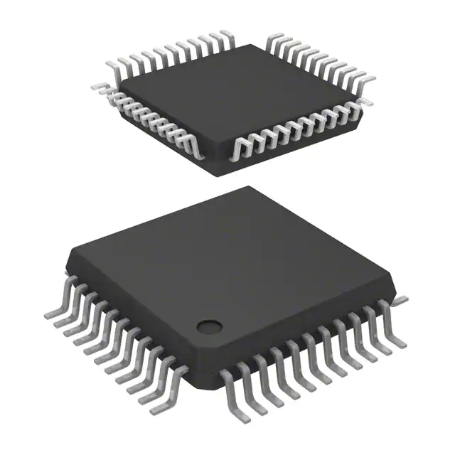
- Part No.:
- TSH511CF
- Manufacturer:
- STMicroelectronics
- Category:
- RF Receivers
- Package:
- 44-LQFP
- Datasheet:
-
 TSH511CF.pdf
- Description:
- RF RX FM 2.3MHZ/2.8MHZ 44TQFP
- Quantity:
- Payment:

- Shipping:

Inventory:2,756
Please send an inquiry. Send us your inquiry, and we will respond immediately.
Product details
Overview
TSH511 from STMicroelectronics is a dual FM analog infrared receiver IC designed for high-fidelity stereo audio reception via infrared carriers. It integrates two independent 0.4–11 MHz FM receivers, each with LNA, intermediate amplifier, limiter, quadrature FM demodulator, and 20 mW audio buffer-enabling direct 16 Ω headphone drive without external amplification. Key confirmed parameters: 4 µV sensitivity @12 dB SINAD, 2.3–5.5 V supply range, and standby-controlled mono operation.
For engineers reviewing the TSH511 datasheet, TSH511 pinout, TSH511 application, or TSH511 equivalent, this device is selected for infrared stereo headsets, subcarrier demodulation in multimedia systems, FM IF receiver design, and power-line carrier intercoms where high input sensitivity, dual-channel RF flexibility, and integrated audio buffering are required.
Technical Context
The TSH511 implements two parallel FM receiver chains sharing a common LNA input stage but featuring independent AMP, limiter, quadrature demodulator, and audio buffer sections. Each chain supports external bandpass/reject filtering at LNA output and AMP output, enabling precise carrier selection (e.g., 2.3 MHz and 2.8 MHz for stereo IR) and interference rejection (e.g., 1.7 MHz microphone TX cancellation).
Its squelch circuit uses a noise rectifier with adjustable threshold (via RMUTE resistor) and ramp-controlled mute timing (14 µA charge / 24 µA discharge on pin 25), while standby pins SBY1/SBY2 allow selective shutdown of RX2 to reduce current from 18 mA (dual active) to 11.5 mA (RX1 active + both buffers on).
Key Specifications
| Parameter | Value and Actual Design Meaning |
|---|---|
| Supply voltage | 2.3 V to 5.5 V - enables single-cell Li-ion or dual-AA battery operation without regulation. |
| Carrier frequency range | 0.4 MHz to 11 MHz - covers standard IR stereo (2.3/2.8 MHz), PLC audio (50–500 kHz), and custom subcarriers. |
| Sensitivity | 4 µV RMS @ 12 dB SINAD - allows direct photodiode connection without preamp in low-light IR environments. |
| Audio output power | 20 mW into 16 Ω - drives stereo headphones directly; eliminates need for external line/headphone amplifiers. |
| LNA gain | 22 dB typical - provides sufficient signal lift before external filtering and limits dynamic range compression risk. |
| Squelch attenuation | 65 dB typical - fully mutes audio during weak-signal conditions, preventing noise burst artifacts. |
| Standby current reduction | From 18 mA to 9.5 mA - achieved by disabling RX2 and its audio buffer, extending battery life in mono mode. |
Pinout & Package
TSH511 is housed in a 44-pin TQFP package (10 × 10 mm, 0.8 mm pitch) with exposed thermal pad for enhanced thermal dissipation in audio-buffer-loaded operation.
| Pin | Circuit Role | Design Meaning |
|---|---|---|
| 1, 7, 13, 21, 27, 33, 35, 43 | GND | Eight dedicated ground connections minimize ground bounce and improve RF/audio separation. |
| 3, 5, 9, 19, 29, 37 | VCC | Six supply pins ensure low-impedance power delivery to RF, analog, and buffer sections independently. |
| 6 | LNA-IN | Common RF input for photodiode; ultra-low-noise (3.4 nV/√Hz) enables direct optical coupling. |
| 31, 32 | SBY1, SBY2 | Digital control inputs to disable RX1/RX2 independently; logic thresholds scale with VCC (0.1×/0.9×). |
| 25 | MUTE-OUT | Ramp generator output controlling mute timing; charges/discharges external capacitor for smooth fade-in/out. |
| 26, 30 | BUF-OUT1, BUF-OUT2 | Class-AB audio outputs capable of 20 mW into 16 Ω; include internal DC-blocking and short-circuit protection. |
Key Features
| Feature | Design Value |
|---|---|
| Dual independent FM receiver chains | Each includes LNA, AMP, limiter, quadrature demodulator, and audio buffer-enabling true stereo IR or mixed-mode (e.g., stereo Rx + mono Tx monitoring). |
| Direct photodiode interface | LNA input noise of 3.4 nV/√Hz and 30 kΩ input impedance allow zero-bias photodiode connection without transimpedance amplifier. |
| Configurable squelch with ramp control | MUTE-OUT pin sources/sinks precise current (14 µA/24 µA) to set attack/release time via external capacitor-eliminates click/pop artifacts. |
| Flexible external filtering access | Dedicated pins (e.g., LNA-OUT1/2, AMP-OUT1/2, MIX-IN1/2) permit insertion of discrete bandpass/reject filters for carrier isolation or EMI suppression. |
| Low-power mono operation | Standby control reduces total ICC from 18 mA to 9.5 mA-critical for battery-powered headsets requiring >10-hour runtime on 2×AA cells. |
Applications
| Infrared Stereo Headphones | Multimedia Headset (Stereo Rx + Mono Tx Monitoring) |
|---|---|
|
Use Scenario: Wireless stereo audio transmission from TV or PC to lightweight headphones using 2.3 MHz and 2.8 MHz infrared carriers. IC Role / Device Role / Timing Role: Dual FM demodulator and audio buffer-receives, demodulates, and drives left/right channels simultaneously with <0.5 µs standby switching. Use Value: Eliminates external amplifiers and power management ICs; 20 mW/channel into 16 Ω meets IEC 60065 loudness requirements without distortion. |
Use Scenario: Bidirectional wireless headset supporting stereo audio playback and voice uplink via separate IR carriers (2.3/2.8 MHz Rx, 1.7 MHz Tx). IC Role / Device Role / Timing Role: Dual-receiver front-end with filter-access pins-enables 1.7 MHz reject filtering on LNA output to suppress microphone TX leakage. Use Value: Prevents self-interference during full-duplex operation; squelch ensures clean muting when voice carrier drops below threshold. |
| Stereo Sub-Carrier Demodulator | Power-Line Carrier Intercom |
|
Use Scenario: Extracting stereo audio from composite video or broadcast signals carrying 5.5 MHz or 6.5 MHz FM subcarriers. IC Role / Device Role / Timing Role: Tunable FM demodulator with wide carrier range (0.4–11 MHz)-configured via external filters to lock onto non-standard subcarriers. Use Value: Replaces discrete PLL+VCO+demodulator designs; 58 dB SNR preserves audio fidelity even under low-SINAD conditions. |
Use Scenario: Two-way voice communication over AC power lines using 50–500 kHz carrier frequencies modulated with voice signals. IC Role / Device Role / Timing Role: High-dynamic-range FM receiver-LNA input handles microvolt-level PLC signals amid high-voltage noise; limiter prevents saturation. Use Value: 127 mVRMS 1dB compression point ensures robust operation in noisy electrical environments without clipping. |
Equivalent & Alternatives
The following parts are listed as comparable options for similar dual FM receiver applications.
| Alternative Part | Technical Difference | Application Difference | Selection Advice |
|---|---|---|---|
| TS4962 | Single-channel FM receiver with integrated Class D amplifier; no LNA or squelch; 3.3 V only. | Supports mono IR audio only; lacks dual-chain architecture and carrier flexibility. | Select only for cost-sensitive mono applications where external LNA and squelch circuitry can be added. |
| MAX9860 | Audio codec with I²S interface and embedded DSP; no RF front-end or FM demodulation capability. | Requires external RF tuner and demodulator; targets digital audio systems, not analog IR receivers. | Choose only if migrating to digital baseband processing and external RF modules are acceptable. |
Compared with TS4962 and MAX9860, the TSH511 uniquely integrates dual analog FM demodulation, ultra-low-noise LNA, and 20 mW headphone drivers in one TQFP package-making it irreplaceable for analog infrared stereo systems requiring minimal BOM count and direct photodiode interfacing.
Availability
TSH511 is available at Aetrix Electronics and suitable for infrared stereo headsets, multimedia wireless headsets, and power-line carrier intercoms requiring stable component supply across extended temperature ranges (−40°C to +85°C) and long-lifecycle support.
Supply support for TSH511 includes scheduled delivery planning, volume procurement assistance, BOM continuity management, traceable sourcing, and lifecycle availability coordination for OEM customers, industrial embedded developers, connected-device designers, and electronics production programs.
Manufacturer
STMicroelectronics is a global semiconductor leader specializing in analog, power, and microcontroller solutions for industrial, automotive, and consumer markets.
The TSH511 belongs to ST's infrared audio receiver product line, engineered specifically for high-sensitivity, low-power stereo IR systems-including TV headsets, PC peripherals, and professional audio intercoms.
FAQ
What is the minimum supply voltage for reliable operation of the TSH511?
The TSH511 operates reliably down to 2.3 V, verified across −40°C to +85°C ambient temperature with full functionality: LNA gain remains stable at 22 dB, squelch threshold holds at 9 mVRMS, and audio buffers deliver ≥15 mW into 16 Ω. Below 2.3 V, LNA noise performance degrades and standby logic thresholds become undefined.
Can the TSH511 demodulate non-standard carrier frequencies like 1.7 MHz or 6.5 MHz?
Yes-the TSH511 supports carrier frequencies from 0.4 MHz to 11 MHz. Its quadrature FM demodulator and external filter access pins (e.g., LNA-OUT1/2, AMP-OUT1/2) enable precise tuning to 1.7 MHz (for voice uplink) or 6.5 MHz (TV sound subcarrier) using discrete LC or ceramic filters, as confirmed in Figures 23 and 24 of the datasheet.
How does the squelch circuit respond to fast signal dropouts?
The squelch uses a ramp generator on MUTE-OUT (pin 25) that charges/discharges an external capacitor with 14 µA/24 µA current. With a 100 nF capacitor, this yields ~7 µs rise/fall time-fast enough to mute noise bursts within one audio cycle at 20 kHz, yet slow enough to avoid chopping speech syllables, as validated in Figure 4's S/N vs. input level curve.
Is thermal management required for continuous 20 mW output per channel?
Yes-under worst-case conditions (VCC = 5.5 V, Tamb = 85°C), the TSH511 dissipates ~110 mW. Its Rthja of 45 °C/W requires either the exposed thermal pad to be soldered to a ≥2 cm² copper pour or forced airflow. Without thermal relief, junction temperature exceeds 150°C after ~3 minutes, triggering thermal shutdown per absolute maximum ratings.
TSH511CF Specifications
- Product attributes
- Attribute value
- Manufacturer:
- STMicroelectronics
- Series:
- -
- Package/Case:
- 44-LQFP
- Packaging:
- Tray
- Product Status:
- Obsolete
- Frequency:
- 2.3MHz ~ 2.8MHz
- Sensitivity:
- -95dBm
- Data Rate (Max):
- -
- Modulation or Protocol:
- FM
- Applications:
- Infrared Headsets, Infrared Hi-Fi Stereo Transmitters
- Current - Receiving:
- 15mA
- Data Interface:
- PCB, Surface Mount
- Memory Size:
- -
- Antenna Connector:
- PCB, Surface Mount
- Features:
- -
- Voltage - Supply:
- 2.3V ~ 5.5V
- Operating Temperature:
- -40°C ~ 85°C
- Grade:
- -
- Qualification:
- -
- Mounting Type:
- Surface Mount
- Supplier Device Package:
- 44-TQFP (10x10)
TSH511CF FAQ
1.How can I place an order for TSH511CF through Aetrix?
Please submit a Request for Quotation (RFQ) for TSH511CF on Aetrix. Our sales agent will provide a competitive quotation and guide you through the order confirmation once you accept the terms.
2.Are the price and stock information for TSH511CF reliable?
The price and inventory of TSH511CF are updated periodically and may fluctuate due to market conditions. Stock and pricing data are typically refreshed every 24 hours. Quotation validity for TSH511CF is usually 5 days.
3.What payment methods are accepted for TSH511CF?
We accept Wire Transfer, PayPal, Credit Card, Western Union, MoneyGram, and Escrow for TSH511CF transactions.
Note: Certain payment methods may incur a processing fee.
4.How is shipping managed for TSH511CF?
TSH511CF orders can be shipped via leading logistics carriers, including DHL, UPS, FedEx, TNT, or Registered Mail.
Once your TSH511CF order is processed, you will receive an email with the shipment details and tracking number.
Note: Tracking information may take up to 24 hours to appear. Express delivery typically takes 3–5 business days.
5.How can I obtain technical support or documentation for TSH511CF?
For technical support, including TSH511CF datasheets, pinout diagrams, or application guidance, please contact our engineering support team. They can provide detailed documentation and assistance for your TSH511CF requirements.
6.How does Aetrix verify that TSH511CF is sourced from the original manufacturer or authorized distributors?
All TSH511CF products on Aetrix are procured from qualified distributors and authorized channels. Our dedicated quality assurance team conducts strict verification, including traceability checks and, if necessary, third-party testing. This ensures that TSH511CF meets industry standards.
7.What is the process for return or replacement of TSH511CF?
All TSH511CF units undergo pre-shipment inspection (PSI). If there is an issue with TSH511CF, returns or replacements are accepted under the following conditions:
1.Quantity discrepancies, incorrect items, or visible external defects (such as breakage or corrosion), acknowledged by Aetrix.
2.The issue is reported within 90 days of delivery.
3.The TSH511CF part is unused and in its original packaging.
Return procedure for TSH511CF:
1.Submit a request within 90 days.
2.Obtain a Return Material Authorization (RMA) from Aetrix.
TSH511CF Tags
-
MICRF220AYQS-TR
Microchip Technology
-
SX1239IMLTRT
Semtech Corporation

-
SI4356-B1A-FMR
Silicon Labs

-
SI4362-C2A-GMR
Silicon Labs

-
MAX1473EUI+T
Analog Devices Inc./Maxim Integrated

-
CMX992Q3
CML Micro

-
CMX994AQ4
CML Micro

-
MAX2112ETI+
Analog Devices Inc./Maxim Integrated
-
MAX2112ETI+T
Analog Devices Inc./Maxim Integrated
-
TESEO-LIV3R
STMicroelectronics
-
M20048-1
Antenova
-
CMX994EQ4
CML Micro
Tech Hub

A practical engineering and sourcing framework covering lifecycle verification, lifetime-buy calculations, replacement qualification, supplier checks and counterfeit-risk controls.

TTL and CMOS logic families differ in thresholds, loading, output drive, power and timing. This engineering guide compares 74HC and 74HCT, calculates noise margins and checks 3.3 V/5 V compatibility.

A practical engineering guide to 3.3V and 5V logic compatibility, input thresholds, resistor dividers, translator ICs, MOSFET level shifting, I2C pull-ups, timing limits and power-sequencing risks.

The 74HC595 uses push-pull logic outputs, while the TPIC6B595 uses 50 V open-drain DMOS sinks for higher-power loads. This guide compares timing, current limits, 3.3 V interfacing, load wiring, thermal…

The 74HC595 converts serial data into eight stable parallel outputs. This guide covers pin functions, shift and storage timing, OE and MR behavior, drive-current limits, cascading, voltage compatibilit…

A technical comparison of level-sensitive latches and edge-triggered flip-flops, covering timing windows, setup and hold limits, master–slave operation, time borrowing, race-through, HDL inference and…

A D latch stores one bit while Enable controls when data can pass. This reference covers gate-level operation, truth tables, transparency, setup and hold timing, LE versus OE, common ICs and practical …

An SR latch stores one bit through cross-coupled feedback. This engineering reference covers NOR and NAND implementations, truth tables, forbidden-state recovery, gated operation, switch debouncing, fa…

Latch circuits retain one bit through feedback. This technical reference covers SR and D latches, truth tables, transparency, timing limits, latch-versus-flip-flop behavior, applications and common log…

An engineering guide to LED driver operation, constant-current and constant-voltage outputs, linear and switching topologies, dimming, IC selection, calculations, replacement compatibility, and fault c…


