
 My Inquiry
 My Account


STMicroelectronics TSM1014AIST
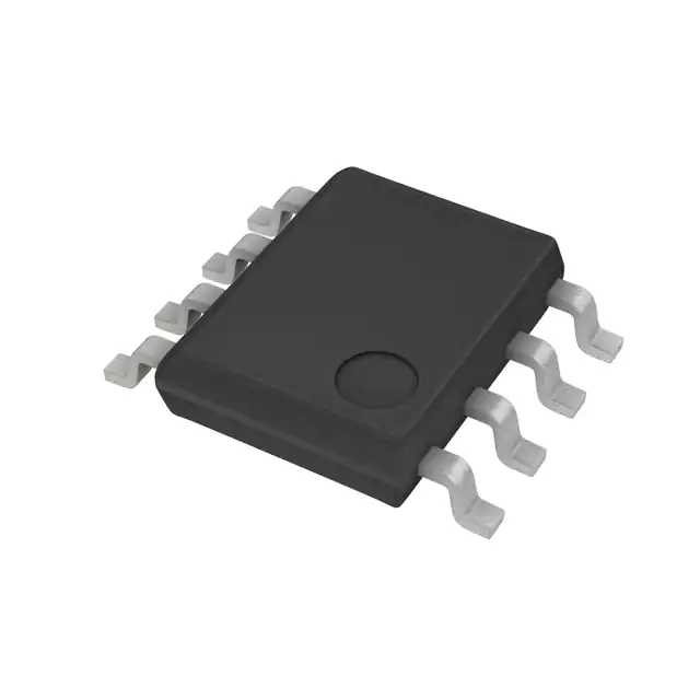
- Part No.:
- TSM1014AIST
- Manufacturer:
- STMicroelectronics
- Category:
- Voltage Reference
- Package:
- 8-TSSOP, 8-MSOP (0.118", 3.00mm Width)
- Datasheet:
-
 TSM1014AIST.pdf
- Description:
- IC VREF SERIES 0.5% 8MINISO
- Quantity:
- Payment:

- Shipping:

Inventory:4,131
Please send an inquiry. Send us your inquiry, and we will respond immediately.
Product details
Overview
TSM1014AIST from STMicroelectronics is a dual operational amplifier-based CV/CC controller IC for secondary-side feedback in flyback SMPS, integrating a 1.25 V ±0.5% voltage reference, two transconductance op-amps (Gm = 0.5–1 mA/mV), 4.5–28 V operation, and 100–180 µA supply current. It enables precise voltage regulation (e.g., 4.1 V output) and current limiting (e.g., battery charge termination) in compact AC/DC adapters and USB-C chargers.
For engineers reviewing the TSM1014AIST datasheet, TSM1014AIST pinout, TSM1014AIST application, or TSM1014AIST equivalent, key selection criteria include its dual-opamp architecture with independent CV/CC loop control, sink-only outputs enabling ORing behavior, 2 kV HBM ESD rating, and MiniSO-8 thermal resistance (180 °C/W) for thermally constrained designs.
Technical Context
The TSM1014AIST implements two independent transconductance operational amplifiers: one configured as a voltage controller (CV) using Vref and pins CV−/CVOUT, and another as a current limiter (CC) using CC−/CC+/CCOUT with external Rsense and resistor divider biasing. Both op-amps feature rail-to-rail input common-mode range (0 to Vcc−1.5 V) and are optimized for optocoupler-driven feedback loops.
Its internal 1.25 V reference (±0.5% at 25°C, ±30 mV over −40 to +105°C) supplies both op-amp bias networks. The sink-only output stage (Ios = 5–10 mA, Vol = 250–400 mV @ 5 mA) eliminates need for external pull-ups and supports direct optocoupler LED drive. Supply rejection (65–100 dB) and low offset drift (7 µV/°C) ensure stability across line and temperature variations.
Key Specifications
| Parameter | Value and Actual Design Meaning |
|---|---|
| Voltage Reference | 1.25 V ±0.5% (TSM1014A variant); enables accurate CV setpoint without external DAC or trimming |
| Supply Voltage Range | 4.5 V to 28 V; supports wide-input universal AC/DC adapters with integrated Zener clamp at 28 V |
| Total Supply Current | 100–180 µA; allows operation from high-impedance auxiliary winding without loading primary side |
| Transconductance Gain | 0.5–1 mA/mV per op-amp; defines current-sink response to 1 mV input differential (e.g., 1 mA sink for 1 mV error) |
| Input Offset Voltage | 0.5 mV (max) for TSM1014A; ensures ≤0.4% current sense error at 100 mV Rsense drop |
| ESD Rating | 2 kV HBM; protects against handling damage during board assembly and test |
| Thermal Resistance | 180 °C/W (Junction-to-Ambient, MiniSO-8); limits self-heating to <10°C rise at 100 µA Icc |
Pinout & Package
Package: MiniSO-8 (plastic micropackage), 3.8 mm × 4.9 mm body, 1.27 mm pitch, 180 °C/W RthJA.
| Pin/Terminal | Circuit Role | Design Meaning |
|---|---|---|
| VRef (Pin 1) | Analog Output | Stable 1.25 V reference source for both CV and CC divider networks; max 2.5 mA sink capability |
| CC− (Pin 2) | Analog Input | Inverting input of current-control op-amp; connected to low-side Rsense terminal for ground-referenced sensing |
| CC+ (Pin 3) | Analog Input | Non-inverting input of current-control op-amp; biased by VRef-derived voltage divider for adjustable Ilim |
| CV− (Pin 4) | Analog Input | Inverting input of voltage-control op-amp; connected to output voltage divider for closed-loop regulation |
| CVOUT (Pin 5) | Analog Output | Sink-only output of voltage-control op-amp; drives optocoupler LED anode via series resistor |
| Gnd (Pin 6) | Power Supply | 0 V reference for all analog signals and internal reference; must be low-impedance connection to power ground |
| CCOUT (Pin 7) | Analog Output | Sink-only output of current-control op-amp; ORed with CVOUT to activate optocoupler under either CV or CC fault |
| Vcc (Pin 8) | Power Supply | Primary supply input (4.5–28 V); includes internal 28 V Zener clamp for transient protection |
Key Features
| Feature | Design Value |
|---|---|
| Dual independent transconductance op-amps | Enables simultaneous, decoupled CV and CC regulation without shared gain stages or cross-coupling errors |
| Integrated 1.25 V precision reference | Eliminates external reference IC and reduces BOM count by one active component in adapter/charger designs |
| Sink-only output architecture | Allows direct optocoupler LED drive without pull-up resistors, reducing PCB area and improving noise immunity |
| Full external compensation access | Both op-amp outputs and inverting inputs exposed for custom pole-zero placement (e.g., 22 kΩ + 2.2 nF networks) |
| High AC mains rejection | 65–100 dB SVR ensures stable regulation despite 50/60 Hz ripple on Vcc derived from rectified auxiliary winding |
Applications
| USB Power Delivery Adapters | Smartphone Fast Chargers |
|---|---|
Use Scenario: 20 W–30 W USB PD 3.0 adapter with programmable voltage (5–9 V) and current (3–3.5 A) profiles. IC Role / Device Role / Timing Role: Secondary-side CV/CC controller providing isolated feedback to primary PWM IC via optocoupler; manages transition between constant-voltage and constant-current phases. Use Value: Enables ±1% output voltage accuracy and ±3% current limit accuracy over full temperature range using only two external resistors per loop. | Use Scenario: 25 W proprietary fast-charging solution for lithium-ion smartphone battery (4.2 V termination, 2.5 A CC phase). IC Role / Device Role / Timing Role: Dual-loop regulator implementing voltage foldback during CC-to-CV transition and precise end-of-charge cutoff. Use Value: Achieves <100 mV output droop during load step (0–2.5 A) due to fast op-amp response and low output impedance sink stage. |
| Laptop AC Adapters | Industrial DC Power Supplies |
Use Scenario: 45 W universal-input laptop adapter with 19.5 V output and overcurrent protection at 2.5 A. IC Role / Device Role / Timing Role: Primary feedback controller managing dynamic load regulation and short-circuit shutdown via ORed CVOUT/CCOUT outputs. Use Value: Delivers <1% line regulation (90–264 VAC input) and <2% load regulation (10–100% load) without secondary-side LDO. | Use Scenario: 36 V/1 A industrial DC power module requiring EN 62368-1 compliance and 1000-hour MTBF. IC Role / Device Role / Timing Role: Isolated secondary-side supervisor ensuring safe current limiting during motor startup surges and cable fault conditions. Use Value: Provides fail-safe current foldback (not just shutdown) with <10 µs response time to Rsense overvoltage events. |
Equivalent & Alternatives
The following parts are listed as comparable options for similar CV/CC controller applications.
| Alternative Part | Technical Difference | Application Difference | Selection Advice |
|---|---|---|---|
| TL431 + LM358 | Discrete solution: separate shunt reference + dual op-amp; no integrated Vref matching or shared thermal tracking | Requires ≥4 external passive components per loop; higher layout sensitivity and calibration effort | Select when legacy design reuse or ultra-low-cost BOM (<$0.12) outweighs footprint and performance benefits |
| UCC28063 | Single-chip PFC + PWM controller with integrated CV/CC; no secondary-side isolation or optocoupler interface | Designed for primary-side regulation only; unsuitable for isolated flyback topologies requiring secondary feedback | Select only for non-isolated buck-derived topologies where primary-side sensing meets safety certification requirements |
Compared with TL431+LM358 and UCC28063, the TSM1014AIST uniquely delivers matched dual op-amps with a common precision reference in a single MiniSO-8 package-enabling compact, thermally stable, optocoupler-based CV/CC control unattainable with discrete or primary-side alternatives.
Availability
TSM1014AIST is available at Aetrix Electronics and suitable for USB PD adapters, smartphone fast chargers, and industrial DC power supplies requiring stable component supply, long-term lifecycle support, and RoHS-compliant MiniSO-8 packaging.
Supply support for TSM1014AIST includes scheduled delivery planning, volume procurement assistance, BOM continuity management, traceable sourcing, and lifecycle availability coordination for OEM customers, industrial embedded developers, connected-device designers, and electronics production programs.
Manufacturer
STMicroelectronics is a global semiconductor leader headquartered in Geneva, Switzerland, designing and manufacturing microcontrollers, power ICs, sensors, and analog products for automotive, industrial, and consumer markets.
The TSM1014 belongs to ST's dedicated SMPS secondary-side controller product line, engineered specifically for cost-sensitive, space-constrained flyback converters needing accurate dual-loop regulation without complex digital control.
FAQ
What is the maximum allowable voltage on the Vcc pin?
The absolute maximum rating for Vcc is 28 V, enforced by an internal Zener clamp. Operation above this voltage risks permanent damage. In practice, Vcc should be limited to ≤27 V under worst-case transient conditions, especially when derived from an auxiliary winding without external clamping.
Can TSM1014AIST drive an optocoupler directly without a series resistor?
No. The sink-output stage requires an external current-limiting resistor between CVOUT/CCOUT and the optocoupler LED anode. For typical PC817-type optocouplers (IF = 5 mA), a 1 kΩ resistor is recommended at Vcc = 12 V to ensure reliable turn-on while staying within the 5–10 mA short-circuit current limit.
How does the 0.5% reference tolerance affect current limit accuracy?
Current limit accuracy depends directly on VRef tolerance because the CC+ input voltage is derived from a resistor divider tied to VRef. With 0.5% VRef tolerance and matched 1% resistors, total current limit error is typically ≤3% over temperature-sufficient for Class II adapter certifications requiring ±5% Ilim.
Is there a recommended PCB layout guideline for minimizing noise coupling into CV− and CC−?
Yes: route CV− and CC− traces away from switching nodes and power planes; use guard rings tied to Gnd around these pins; place the VRef bypass capacitor (100 nF X7R) within 2 mm of Pin 1; and avoid sharing Gnd return paths between Rsense and output voltage dividers to prevent common-impedance coupling.
TSM1014AIST Specifications
- Product attributes
- Attribute value
- Manufacturer:
- STMicroelectronics
- Package/Case:
- 8-TSSOP, 8-MSOP (0.118", 3.00mm Width)
- Series:
- -
- Packaging:
- Tape & Reel (TR)
- Product Status:
- Obsolete
- Reference Type:
- Series
- Output Type:
- Fixed
- Voltage - Output (Min/Fixed):
- 1.25V
- Voltage - Output (Max):
- -
- Current - Output:
- 2.5 mA
- Tolerance:
- ±0.5%
- Temperature Coefficient:
- -
- Noise - 0.1Hz to 10Hz:
- -
- Noise - 10Hz to 10kHz:
- -
- Voltage - Input:
- 4.5V ~ 28V
- Current - Supply:
- 50mA
- Current - Cathode:
- -
- Operating Temperature:
- -40°C ~ 105°C (TA)
- Grade:
- -
- Qualification:
- -
- Mounting Type:
- Surface Mount
- Supplier Device Package:
- 8-MiniSO
TSM1014AIST FAQ
1.How can I place an order for TSM1014AIST through Aetrix?
Please submit a Request for Quotation (RFQ) for TSM1014AIST on Aetrix. Our sales agent will provide a competitive quotation and guide you through the order confirmation once you accept the terms.
2.Are the price and stock information for TSM1014AIST reliable?
The price and inventory of TSM1014AIST are updated periodically and may fluctuate due to market conditions. Stock and pricing data are typically refreshed every 24 hours. Quotation validity for TSM1014AIST is usually 5 days.
3.What payment methods are accepted for TSM1014AIST?
We accept Wire Transfer, PayPal, Credit Card, Western Union, MoneyGram, and Escrow for TSM1014AIST transactions.
Note: Certain payment methods may incur a processing fee.
4.How is shipping managed for TSM1014AIST?
TSM1014AIST orders can be shipped via leading logistics carriers, including DHL, UPS, FedEx, TNT, or Registered Mail.
Once your TSM1014AIST order is processed, you will receive an email with the shipment details and tracking number.
Note: Tracking information may take up to 24 hours to appear. Express delivery typically takes 3–5 business days.
5.How can I obtain technical support or documentation for TSM1014AIST?
For technical support, including TSM1014AIST datasheets, pinout diagrams, or application guidance, please contact our engineering support team. They can provide detailed documentation and assistance for your TSM1014AIST requirements.
6.How does Aetrix verify that TSM1014AIST is sourced from the original manufacturer or authorized distributors?
All TSM1014AIST products on Aetrix are procured from qualified distributors and authorized channels. Our dedicated quality assurance team conducts strict verification, including traceability checks and, if necessary, third-party testing. This ensures that TSM1014AIST meets industry standards.
7.What is the process for return or replacement of TSM1014AIST?
All TSM1014AIST units undergo pre-shipment inspection (PSI). If there is an issue with TSM1014AIST, returns or replacements are accepted under the following conditions:
1.Quantity discrepancies, incorrect items, or visible external defects (such as breakage or corrosion), acknowledged by Aetrix.
2.The issue is reported within 90 days of delivery.
3.The TSM1014AIST part is unused and in its original packaging.
Return procedure for TSM1014AIST:
1.Submit a request within 90 days.
2.Obtain a Return Material Authorization (RMA) from Aetrix.
TSM1014AIST Tags
-
TL431AIDBZR
Texas Instruments
-
TL431BQDBZR
Texas Instruments

-
AN431AN-ATRG1
Diodes Incorporated
-
LM4040CYM3-2.5-TR
Microchip Technology
-
LM4040CYM3-4.1-TR
Microchip Technology
-
LM4040EIM3-2.5/NOPB
Texas Instruments
-
AZ431LBNTR-G1
Diodes Incorporated
-
LM4040D20IDBZR
Texas Instruments
-
LM4041DIM3-ADJ/NOPB
Texas Instruments
-
LM4040DIM3X-2.5/NOPB
Texas Instruments
-
LM4040DIM3-2.5/NOPB
Texas Instruments
-
AZ431LANTR-G1
Diodes Incorporated
Tech Hub

A practical engineering and sourcing framework covering lifecycle verification, lifetime-buy calculations, replacement qualification, supplier checks and counterfeit-risk controls.

TTL and CMOS logic families differ in thresholds, loading, output drive, power and timing. This engineering guide compares 74HC and 74HCT, calculates noise margins and checks 3.3 V/5 V compatibility.

A practical engineering guide to 3.3V and 5V logic compatibility, input thresholds, resistor dividers, translator ICs, MOSFET level shifting, I2C pull-ups, timing limits and power-sequencing risks.

The 74HC595 uses push-pull logic outputs, while the TPIC6B595 uses 50 V open-drain DMOS sinks for higher-power loads. This guide compares timing, current limits, 3.3 V interfacing, load wiring, thermal…

The 74HC595 converts serial data into eight stable parallel outputs. This guide covers pin functions, shift and storage timing, OE and MR behavior, drive-current limits, cascading, voltage compatibilit…

A technical comparison of level-sensitive latches and edge-triggered flip-flops, covering timing windows, setup and hold limits, master–slave operation, time borrowing, race-through, HDL inference and…

A D latch stores one bit while Enable controls when data can pass. This reference covers gate-level operation, truth tables, transparency, setup and hold timing, LE versus OE, common ICs and practical …

An SR latch stores one bit through cross-coupled feedback. This engineering reference covers NOR and NAND implementations, truth tables, forbidden-state recovery, gated operation, switch debouncing, fa…

Latch circuits retain one bit through feedback. This technical reference covers SR and D latches, truth tables, transparency, timing limits, latch-versus-flip-flop behavior, applications and common log…

An engineering guide to LED driver operation, constant-current and constant-voltage outputs, linear and switching topologies, dimming, IC selection, calculations, replacement compatibility, and fault c…


