
 My Inquiry
 My Account


Texas Instruments TUSB213QRGYTQ1
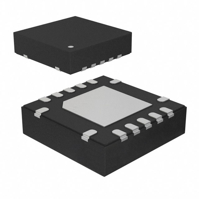
- Part No.:
- TUSB213QRGYTQ1
- Manufacturer:
- Texas Instruments
- Category:
- Specialized
- Package:
- 14-VFQFN Exposed Pad
- Datasheet:
-
 TUSB213QRGYTQ1.pdf
- Description:
- IC INTERFACE SPECIALIZED 14VQFN
- Quantity:
- Payment:

- Shipping:

Inventory:268
Please send an inquiry. Send us your inquiry, and we will respond immediately.
Product details
Overview
TUSB213QRGYTQ1 from Texas Instruments is an automotive-qualified USB 2.0 High-Speed signal conditioner IC designed to compensate for inter-symbol interference (ISI) loss in transmission channels. It supports LS/FS/HS signaling, provides programmable AC and DC boost (4 AC levels, 3 DC levels), operates from 4.4 V to 5.5 V, and delivers 30 mA typical active current at 480 Mbps - enabling reliable USB HS compliance in infotainment head units with long PCB traces or cable extensions.
For engineers reviewing the TUSB213QRGYTQ1 datasheet, TUSB213QRGYTQ1 pinout, TUSB213QRGYTQ1 application, or TUSB213QRGYTQ1 equivalent, key selection considerations include its AEC-Q100 Grade 2 qualification (–40°C to 105°C), host/device-agnostic D1P/D1M and D2P/D2M port interchangeability, ultra-low 0.76 mA HS suspend current, and I²C-configurable operation (address 0x2C) for dynamic tuning of signal integrity parameters.
Technical Context
The TUSB213QRGYTQ1 implements a patent-pending signal conditioning architecture that preserves LS and FS signal characteristics while applying adaptive equalization exclusively to HS differential pairs. Its dual-path design allows flexible placement - near the connector to pass USB near-end eye mask or near the PHY to improve far-end integrity.
Configuration is supported via pin-strapping (EQ for AC boost, DC_BOOST for DC gain) or I²C interface, with latched settings sampled on RSTN de-assertion. The device outputs status flags (CD for connection detection, ENA_HS for HS mode assertion) and supplies a regulated 1.8-V VREG output for internal core logic when active.
Key Specifications
| Parameter | Value and Actual Design Meaning |
|---|---|
| Supply Voltage | 4.4 V to 5.5 V - compatible with standard USB VBUS without external regulation |
| Operating Temperature | –40°C to 105°C ambient - meets AEC-Q100 Grade 2 for automotive cabin environments |
| HS Active Current | 30 mA typical at 480 Mbps - enables low-power operation in always-on infotainment systems |
| HS Suspend Current | 0.76 mA typical - minimizes standby power draw during USB link suspension |
| AC Boost Levels | 4 selectable settings via EQ pin pulldown resistor - fine-tunes high-frequency gain to restore eye opening |
| DC Boost Levels | 3 settings (40/60/80 mV) via DC_BOOST pin strap - compensates for low-frequency attenuation from cables/traces |
| I²C Address | 0x2C - enables runtime reconfiguration and status readback without hardware changes |
Pinout & Package
VQFN-14 (RGY) package, 3.5 mm × 3.5 mm, 1 mm max height, with exposed thermal pad requiring PCB soldering for thermal and mechanical performance.
| Pin/Terminal | Circuit Role | Design Meaning |
|---|---|---|
| EQ | AC boost configuration input | Four-level AC gain selection via external pulldown resistor; sampled once at reset |
| D1P / D1M / D2P / D2M | HS differential I/O ports | Interchangeable host/device-agnostic lanes; support bidirectional HS signal conditioning |
| DC_BOOST/ENA_HS | Configurable I/O | Tri-level DC gain control at reset; becomes HS mode flag (ENA_HS) post-reset |
| SCL/CD | I²C clock / connection detect output | Configurable as I²C clock or open-drain CD flag indicating USB attachment state |
| SDA | I²C data I/O | Bidirectional I²C data line (address 0x2C); used for register read/write and status monitoring |
| RSTN | Active-low enable/reset | Asynchronous shutdown control; must be held low until VCC stabilizes ≥4.4 V |
| VREG | 1.8-V LDO output | Supplies internal core logic only during HS mode; requires 0.1-µF decoupling to GND |
Key Features
| Feature | Design Value |
|---|---|
| AEC-Q100 Grade 2 qualification | Validated for –40°C to 105°C ambient operation in automotive infotainment and telematics modules |
| LS/FS transparent signal path | No alteration of low/full-speed USB signaling - ensures backward compatibility without protocol impact |
| Daisy-chain capability | Enables cascaded deployment for high-loss channels exceeding 5 m pre-channel or 2 m post-channel cable length |
| Ultra-low HS suspend power | 0.76 mA typical current draw maintains USB link state while minimizing system-level quiescent load |
| Programmable AC + DC boost | Independent tuning of high- and low-frequency gain restores USB HS eye diagram integrity per USB-IF compliance tests |
Applications
| Automotive Infotainment Head Unit | Notebook Docking Station |
|---|---|
Use Scenario: Long PCB traces between USB controller and rear-panel Type-A receptacle cause HS signal degradation failing USB-IF near-end eye mask. IC Role / Device Role / Timing Role: Signal conditioner placed adjacent to connector to restore differential eye opening and jitter margin. Use Value: Enables pass/fail compliance testing at production without redesigning layout or adding expensive active cables. | Use Scenario: Docking station with multiple downstream USB ports experiences marginal HS signal integrity due to trace splits and connector losses. IC Role / Device Role / Timing Role: TUSB213QRGYTQ1 deployed per-port to condition each HS lane independently before reaching the receptacle. Use Value: Guarantees stable enumeration and 480 Mbps throughput across all ports under varying cable and peripheral loads. |
| Industrial Tablet USB Host Port | Automotive Active Cable Extender |
Use Scenario: Ruggedized tablet with integrated USB host must drive 2 m active cable to external peripherals in harsh EMI environments. IC Role / Device Role / Timing Role: Signal conditioner placed at tablet's USB PHY output to pre-compensate for cable-induced loss before transmission. Use Value: Maintains HS link reliability over full temperature range and vibration conditions without firmware intervention. | Use Scenario: Automotive-grade USB extension cable requires embedded signal regeneration to meet OEM HS timing budgets over 5 m length. IC Role / Device Role / Timing Role: TUSB213QRGYTQ1 integrated into cable assembly's inline module to boost both AC and DC components of HS signal. Use Value: Eliminates need for costly retimers or custom ASICs while achieving AEC-Q100-compliant performance. |
Equivalent & Alternatives
The following parts are listed as comparable options for similar USB 2.0 signal conditioning applications.
| Alternative Part | Technical Difference | Application Difference | Selection Advice |
|---|---|---|---|
| TS3USB221AIPWR | Passive 2-channel USB 2.0 switch with 6 Ω on-resistance; no signal conditioning or boost capability | Used for USB port multiplexing, not signal restoration; lacks HS equalization, DC/AC boost, or automotive qualification | Select only when channel switching-not signal integrity enhancement-is required |
| MAX3353EETA+ | USB 2.0 transceiver with integrated ESD protection (±15 kV HBM); no equalization, boost, or AEC-Q100 rating | Designed for basic physical layer interface with robust ESD tolerance; no compensation for ISI or cable loss | Choose for cost-sensitive non-automotive designs where signal loss is negligible and ESD is primary concern |
Compared with TS3USB221AIPWR and MAX3353EETA+, the TUSB213QRGYTQ1 uniquely delivers programmable AC/DC boost, AEC-Q100 qualification, and USB-IF HS compliance support - making it the only viable option for automotive or long-channel USB 2.0 signal restoration where passive switches or basic transceivers fail to meet eye mask requirements.
Availability
TUSB213QRGYTQ1 is available at Aetrix Electronics and suitable for automotive infotainment systems, notebook docking stations, and industrial tablet USB host interfaces requiring stable component supply across extended temperature ranges and long production lifecycles.
Supply support for TUSB213QRGYTQ1 includes scheduled delivery planning, volume procurement assistance, BOM continuity management, traceable sourcing, and lifecycle availability coordination for OEM customers, industrial embedded developers, connected-device designers, and electronics production programs.
Manufacturer
Texas Instruments is a global semiconductor company delivering analog and embedded processing solutions for automotive, industrial, personal electronics, and communications markets.
The TUSB213-Q1 product line was developed specifically to address USB 2.0 High-Speed signal integrity challenges in automotive-grade systems, supporting AEC-Q100 compliance and seamless integration into infotainment, telematics, and body electronics platforms.
FAQ
What is the primary function of the TUSB213QRGYTQ1 in a USB 2.0 system?
The TUSB213QRGYTQ1 functions as a High-Speed signal conditioner that compensates for inter-symbol interference (ISI) and channel loss in USB 2.0 links. It applies programmable AC and DC boost to restore differential eye opening without altering LS/FS signals. This enables reliable USB-IF electrical compliance testing at the connector - especially critical in automotive infotainment systems with long PCB traces or extended cables. The TUSB213QRGYTQ1 does not act as a switch, transceiver, or hub controller.
How does the TUSB213QRGYTQ1 handle Low Speed and Full Speed USB traffic?
The TUSB213QRGYTQ1 is explicitly designed to be transparent to Low Speed (1.5 Mbps) and Full Speed (12 Mbps) USB signaling. Its patent-pending architecture bypasses LS/FS signals without modification, preserving their voltage levels, timing, and waveform integrity. Only High Speed (480 Mbps) differential pairs undergo equalization. This ensures full backward compatibility with legacy USB devices while delivering targeted signal restoration where needed - a key requirement validated in the TUSB213QRGYTQ1 datasheet Section 7.1.
Can the TUSB213QRGYTQ1 be configured after power-up without resetting the device?
No. Configuration changes to AC boost (via EQ pin) or DC boost (via DC_BOOST pin) require toggling the RSTN pin to re-latch settings. The TUSB213QRGYTQ1 samples these pins only upon de-assertion of RSTN and ignores real-time adjustments thereafter. For dynamic tuning without hardware reset, the I²C interface (address 0x2C) must be used to write to registers ACB_LVL (0x01) and DCB_LVL (0x0E), followed by clearing CFG_ACTIVE (0x03) to restart the state machine - as specified in the TUSB213QRGYTQ1 register map.
What is the role of the VREG pin on the TUSB213QRGYTQ1?
The VREG pin on the TUSB213QRGYTQ1 is a 1.8-V LDO output that powers the internal digital core logic exclusively during High Speed mode operation. It is not active in LS/FS modes or shutdown. A mandatory 0.1-µF ceramic capacitor must be placed between VREG and GND to stabilize this output. This pin is not intended for external circuitry power; using it as such may compromise TUSB213QRGYTQ1 functionality or violate absolute maximum ratings.
Is the TUSB213QRGYTQ1 compatible with USB On-The-Go (OTG) and Battery Charging (BC) protocols?
Yes. The TUSB213QRGYTQ1 is explicitly qualified for compatibility with USB On-The-Go (OTG) 2.0 and Battery Charging (BC) 1.2 specifications, as stated in its official features list and Section 3 of the datasheet. Its host/device-agnostic D1P/D1M and D2P/D2M port configuration supports bidirectional OTG negotiation, while its transparent LS/FS path ensures BC detection logic (e.g., D+ pull-up recognition) remains unaltered - enabling correct charger identification and current negotiation in automotive and portable applications using the TUSB213QRGYTQ1.
TUSB213QRGYTQ1 Specifications
- Product attributes
- Attribute value
- Manufacturer:
- Texas Instruments
- Series:
- -
- Package/Case:
- 14-VFQFN Exposed Pad
- Packaging:
- Tape & Reel (TR)
- Product Status:
- Active
- Applications:
- Signal Processing
- Interface:
- USB
- Voltage - Supply:
- 4.4V ~ 5.5V
- Supplier Device Package:
- 14-VQFN (3.5x3.5)
- Grade:
- Automotive
- Qualification:
- AEC-Q100
- Mounting Type:
- Surface Mount
TUSB213QRGYTQ1 FAQ
1.How can I place an order for TUSB213QRGYTQ1 through Aetrix?
Please submit a Request for Quotation (RFQ) for TUSB213QRGYTQ1 on Aetrix. Our sales agent will provide a competitive quotation and guide you through the order confirmation once you accept the terms.
2.Are the price and stock information for TUSB213QRGYTQ1 reliable?
The price and inventory of TUSB213QRGYTQ1 are updated periodically and may fluctuate due to market conditions. Stock and pricing data are typically refreshed every 24 hours. Quotation validity for TUSB213QRGYTQ1 is usually 5 days.
3.What payment methods are accepted for TUSB213QRGYTQ1?
We accept Wire Transfer, PayPal, Credit Card, Western Union, MoneyGram, and Escrow for TUSB213QRGYTQ1 transactions.
Note: Certain payment methods may incur a processing fee.
4.How is shipping managed for TUSB213QRGYTQ1?
TUSB213QRGYTQ1 orders can be shipped via leading logistics carriers, including DHL, UPS, FedEx, TNT, or Registered Mail.
Once your TUSB213QRGYTQ1 order is processed, you will receive an email with the shipment details and tracking number.
Note: Tracking information may take up to 24 hours to appear. Express delivery typically takes 3–5 business days.
5.How can I obtain technical support or documentation for TUSB213QRGYTQ1?
For technical support, including TUSB213QRGYTQ1 datasheets, pinout diagrams, or application guidance, please contact our engineering support team. They can provide detailed documentation and assistance for your TUSB213QRGYTQ1 requirements.
6.How does Aetrix verify that TUSB213QRGYTQ1 is sourced from the original manufacturer or authorized distributors?
All TUSB213QRGYTQ1 products on Aetrix are procured from qualified distributors and authorized channels. Our dedicated quality assurance team conducts strict verification, including traceability checks and, if necessary, third-party testing. This ensures that TUSB213QRGYTQ1 meets industry standards.
7.What is the process for return or replacement of TUSB213QRGYTQ1?
All TUSB213QRGYTQ1 units undergo pre-shipment inspection (PSI). If there is an issue with TUSB213QRGYTQ1, returns or replacements are accepted under the following conditions:
1.Quantity discrepancies, incorrect items, or visible external defects (such as breakage or corrosion), acknowledged by Aetrix.
2.The issue is reported within 90 days of delivery.
3.The TUSB213QRGYTQ1 part is unused and in its original packaging.
Return procedure for TUSB213QRGYTQ1:
1.Submit a request within 90 days.
2.Obtain a Return Material Authorization (RMA) from Aetrix.
TUSB213QRGYTQ1 Tags

-
NVT4857UKAZ
NXP Semiconductors

-
TCA8418RTWR
Texas Instruments

-
PCA9546APWR
Texas Instruments

-
MD0100N8-G
Microchip Technology

-
PCA9548APW,118
NXP Semiconductors

-
PCA9540BDP,118
NXP Semiconductors

-
PCA9548APWR
Texas Instruments

-
PCA9546APW,118
NXP Semiconductors

-
PTN3360DBS,518
NXP Semiconductors

-
PCA9546ABS,118
NXP Semiconductors

-
PCA9518PWR
Texas Instruments

-
PCA9545APW,118
NXP Semiconductors
Tech Hub

A practical engineering guide to 3.3V and 5V logic compatibility, input thresholds, resistor dividers, translator ICs, MOSFET level shifting, I2C pull-ups, timing limits and power-sequencing risks.

The 74HC595 uses push-pull logic outputs, while the TPIC6B595 uses 50 V open-drain DMOS sinks for higher-power loads. This guide compares timing, current limits, 3.3 V interfacing, load wiring, thermal…

The 74HC595 converts serial data into eight stable parallel outputs. This guide covers pin functions, shift and storage timing, OE and MR behavior, drive-current limits, cascading, voltage compatibilit…

A technical comparison of level-sensitive latches and edge-triggered flip-flops, covering timing windows, setup and hold limits, master–slave operation, time borrowing, race-through, HDL inference and…

A D latch stores one bit while Enable controls when data can pass. This reference covers gate-level operation, truth tables, transparency, setup and hold timing, LE versus OE, common ICs and practical …

An SR latch stores one bit through cross-coupled feedback. This engineering reference covers NOR and NAND implementations, truth tables, forbidden-state recovery, gated operation, switch debouncing, fa…

Latch circuits retain one bit through feedback. This technical reference covers SR and D latches, truth tables, transparency, timing limits, latch-versus-flip-flop behavior, applications and common log…

An engineering guide to LED driver operation, constant-current and constant-voltage outputs, linear and switching topologies, dimming, IC selection, calculations, replacement compatibility, and fault c…

Operational amplifier guide covering op amp basics, feedback, ideal vs real op amps, common configurations, buffer circuits, offset, bias current, gain-bandwidth, slew rate, rail-to-rail limits and sel…

Jumper cables guide covering safe connection order, red and black clamp placement, final ground connection, cable gauge, length, clamp quality, copper vs CCA cables, jump starter comparison and battery…


