
 My Inquiry
 My Account


Texas Instruments TUSB4020BIPHPRQ1
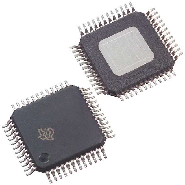
- Part No.:
- TUSB4020BIPHPRQ1
- Manufacturer:
- Texas Instruments
- Category:
- Controllers
- Package:
- 48-PowerTQFP
- Datasheet:
-
 TUSB4020BIPHPRQ1.pdf
- Description:
- IC USB 2.0 2PORT HUB IND 48HTQFP
- Quantity:
- Payment:

- Shipping:

Inventory:1,595
Please send an inquiry. Send us your inquiry, and we will respond immediately.
Product details
Overview
TUSB4020BIPHPRQ1 from Texas Instruments is an AEC-Q100 Grade-3 qualified two-port USB 2.0 hub IC for automotive systems, supporting high-speed (480 Mbps), full-speed (12 Mbps), and low-speed (1.5 Mbps) upstream/downstream connectivity, per-port or ganged power switching, and battery charging modes (CDP/DCP/YD/T 1591-2009 compliant) in a 48-pin HTQFP package.
For engineers reviewing the TUSB4020BIPHPRQ1 datasheet, TUSB4020BIPHPRQ1 pinout, TUSB4020BIPHPRQ1 application, or TUSB4020BIPHPRQ1 equivalent, key selection criteria include automotive temperature range (–40°C to 85°C), MTT architecture with four endpoint buffers per translator, 24 MHz clock input support, I²C/SMBus/OTP configurability, and USB Type-C compatibility with integrated VBUS monitoring and battery charging control logic.
Technical Context
The TUSB4020BIPHPRQ1 implements a Multi-Transaction Translator (MTT) hub architecture with two independent transaction translators and four asynchronous endpoint buffers per translator, enabling concurrent high-bandwidth transfers across downstream ports. It supports dynamic speed negotiation: high-speed operation on downstream ports is enabled only when the upstream port detects a high-speed capable host.
Power management is configurable via hardware strapping (GANGED, FULLPWRMGMTz, PWRCTL_POL) or register control, supporting both individual port power switching (with isolated overcurrent shutdown) and ganged operation (simultaneous power enable/disable). Battery charging mode selection (CDP, DCP, divider) is determined at reset by BATEN pins and register settings, with AUTOMODE enabling automatic DCP/divider switching based on attached device detection.
Key Specifications
| Parameter | Value and Actual Design Meaning |
|---|---|
| USB Compliance | USB 2.0 specification compliant; supports high-speed (480 Mbps), full-speed (12 Mbps), and low-speed (1.5 Mbps) signaling on all ports. |
| Operating Temperature | AEC-Q100 Grade 3: –40°C to +85°C ambient, validated for automotive cabin and infotainment environments. |
| Supply Voltages | VDD = 1.1 V ±10% (core), VDD33 = 3.3 V ±10% (I/O); no strict power sequencing required between rails. |
| Power Management | Per-port or ganged power switching with dedicated OVERCUR1z/OVERCUR2z inputs; active-high/active-low polarity selectable via PWRCTL_POL. |
| Battery Charging | CDP mode (upstream connected), DCP mode (upstream unconnected, YD/T 1591-2009 compliant), and D+/D– divider mode; AUTOMODE enables automatic mode selection. |
| Configuration Interface | OTP ROM, I²C EEPROM (100 kbps, address 0x50), or SMBus target interface (7-bit address 0x88–0x8F) for VID/PID, port customization, and string programming. |
| Crystal Input | 24 MHz fundamental-mode crystal supported on XI/XO pins; external oscillator input also accepted on XI with XO left floating. |
Pinout & Package
Package: 48-pin HTQFP (PHP), 9 mm × 9 mm body, exposed thermal pad, RoHS-compliant.
| Pin/Terminal | Circuit Role | Design Meaning |
|---|---|---|
| GRSTz (11) | Global Reset Input | Active-low asynchronous reset; forces all internal registers to default state; must be held low ≥3 ms after supplies stabilize. |
| USB_DP_UP / USB_DM_UP (26, 27) | Upstream Differential Pair | High-speed USB 2.0 transceiver interface to host controller; requires 90 Ω differential impedance routing. |
| USB_DP_DN1 / USB_DM_DN1 (41, 42) | Downstream Port 1 Pair | Full-speed/low-speed/high-speed transceiver for peripheral connection; supports hot-plug detection and suspend/resume signaling. |
| PWRCTL1/BATEN1 (4) | Port 1 Power/Battery Control | Configures port 1 power switch enable and battery charging support (0 = disabled, 1 = enabled) sampled at reset deassertion. |
| OVERCUR1z (5) | Port 1 Overcurrent Sense | Active-low input tied to external power switch fault output; triggers port-specific power disable in individual mode or hub-wide disable in ganged mode. |
| SCL/SMBCLK (2) & SDA/SMBDAT (3) | I²C/SMBus Interface | Selectable via SMBUSz pin: I²C EEPROM (SMBUSz=1) or SMBus target (SMBUSz=0); used for runtime configuration and firmware updates. |
| GANGED/SMBA2/HS_UP (35) | Mode Selection Input | Determines power control topology (0 = per-port, 1 = ganged) and reports upstream high-speed link status post-reset. |
| FULLPWRMGMTz/SMBA1 (36) | Power Management Enable | Enables/disables downstream port power switching (0 = enabled, 1 = disabled); also sets SMBus address bit 1 when SMBUSz=0. |
Key Features
| Feature | Design Value |
|---|---|
| AEC-Q100 Grade 3 Qualification | Validated for automotive use with guaranteed operation from –40°C to +85°C ambient and robust ESD immunity (±4 kV HBM). |
| Multi-Transaction Translator (MTT) | Two independent transaction translators with four asynchronous endpoint buffers each, eliminating bandwidth contention between downstream ports. |
| Type-C Compatibility & VBUS Monitoring | Integrated USB_VBUS sense input with precision resistor divider (90.9kΩ + 10kΩ) enables reliable upstream port presence and power source detection. |
| Flexible Battery Charging Support | Hardware-configurable CDP/DCP/divider modes per port, including YD/T 1591-2009 compliance and AUTOMODE for automatic charger identification without host intervention. |
| Triple Configuration Options | One-time programmable (OTP) ROM for factory-set VID/PID/port attributes, plus field-upgradable I²C EEPROM or SMBus target interface for runtime customization of strings, serial numbers, and PHY settings. |
Applications
| Automotive Infotainment Hub | Front Console USB Expansion |
|---|---|
Use Scenario: Integrating multiple USB peripherals (e.g., smartphone, SD card reader, USB audio device) into a vehicle's front console while maintaining AEC-Q100 compliance. IC Role / Device Role / Timing Role: USB 2.0 hub IC providing high-speed data aggregation, per-port power control, and battery charging negotiation for connected devices. Use Value: Enables single upstream USB connection to head unit while delivering up to 500 mA per downstream port with overcurrent protection and automotive-grade reliability. | Use Scenario: Adding dual USB-A ports to a vehicle's center stack for passenger convenience, supporting simultaneous charging and data transfer. IC Role / Device Role / Timing Role: Automotive-qualified USB hub managing power delivery, speed negotiation, and charger detection across two downstream ports. Use Value: Eliminates need for discrete power switches and level shifters; built-in DCP/CDP support ensures fast charging for smartphones without host software involvement. |
| Automotive Docking Station | Telematics Module Interface |
Use Scenario: Enabling plug-and-play connectivity for diagnostic tools, firmware update dongles, and wireless tethering adapters in service bay docking stations. IC Role / Device Role / Timing Role: Robust USB 2.0 hub with ganged power control and SMBus configuration interface for secure, field-programmable peripheral attachment. Use Value: Supports hot-plug detection and suspend/resume across all ports; SMBus target mode allows telematics gateway to reconfigure hub parameters remotely during vehicle OTA updates. | Use Scenario: Interfacing USB-based GNSS receivers, cellular modems, and CAN-to-USB gateways within an automotive telematics control unit (TCU). IC Role / Device Role / Timing Role: High-integrity USB hub ensuring deterministic latency, ESD-hardened signal paths, and stable power delivery in electrically noisy vehicle networks. Use Value: MTT architecture prevents data starvation between GNSS and modem traffic; 125°C max junction temperature rating ensures operation under hood-adjacent mounting conditions. |
Equivalent & Alternatives
The following parts are listed as comparable options for similar USB 2.0 hub applications.
| Alternative Part | Technical Difference | Application Difference | Selection Advice |
|---|---|---|---|
| TUSB4041IPRQ1 | Four-port USB 2.0 hub with identical MTT architecture, AEC-Q100 Grade 3 rating, and same 48-pin HTQFP package; adds third downstream port and additional configuration flexibility. | Requires PCB layout change for extra port routing; suitable when system needs >2 downstream connections without cascading hubs. | Select when expanding peripheral count beyond two ports while retaining automotive qualification and power management features. |
| USB2514B-AEZG-TR | Four-port USB 2.0 hub with MTT, but commercial-grade (–40°C to +85°C not AEC-Q100 certified); uses 48-pin QFN instead of HTQFP; lacks automotive-specific battery charging modes (YD/T 1591-2009). | Not qualified for automotive safety-critical or long-lifecycle deployments; limited to industrial or consumer docking applications. | Consider only for non-automotive designs where cost is prioritized over qualification, and battery charging compliance is unnecessary. |
Compared with TUSB4020BIPHPRQ1, the TUSB4041IPRQ1 offers scalable port count with identical automotive reliability and feature set, whereas the USB2514B-AEZG-TR provides higher port density at lower cost but sacrifices AEC-Q100 validation and automotive-specific charging protocols-making it unsuitable for production vehicle ECUs.
Availability
TUSB4020BIPHPRQ1 is available at Aetrix Electronics and suitable for automotive infotainment systems, front console USB expansion, and telematics module interfaces requiring stable component supply, long-term lifecycle support, and AEC-Q100 compliance.
Supply support for TUSB4020BIPHPRQ1 includes scheduled delivery planning, volume procurement assistance, BOM continuity management, traceable sourcing, and lifecycle availability coordination for OEM customers, industrial embedded developers, connected-device designers, and electronics production programs.
Manufacturer
Texas Instruments is a global semiconductor company specializing in analog, embedded processing, and connectivity technologies, with leadership in automotive-grade ICs and USB interface solutions.
The TUSB4020BIPHPRQ1 belongs to TI's automotive-qualified USB hub product line, designed specifically for robust, low-latency USB 2.0 expansion in vehicles-emphasizing AEC-Q100 compliance, battery charging interoperability, and flexible configuration for diverse ECU architectures.
FAQ
What is the operating temperature range for the TUSB4020BIPHPRQ1?
The TUSB4020BIPHPRQ1 is AEC-Q100 Grade 3 qualified and operates from –40°C to +85°C ambient temperature. This range is validated for automotive cabin and infotainment applications, with junction temperature rated up to 105°C under normal operation and 125°C absolute maximum. Thermal design must account for RθJA = 31.8°C/W in the 48-pin HTQFP package.
Does the TUSB4020BIPHPRQ1 support USB Type-C connectors directly?
The TUSB4020BIPHPRQ1 is Type-C compatible but does not integrate native USB Type-C PHY or CC logic. It supports Type-C implementations via external multiplexers and CC detection circuits; its USB_DP/DM signals connect to standard USB 2.0 lanes routed through a Type-C receptacle. The device's VBUS monitoring and battery charging features align with Type-C power delivery expectations.
How is battery charging configured on the TUSB4020BIPHPRQ1?
Battery charging on the TUSB4020BIPHPRQ1 is configured via hardware strapping (PWRCTL1/BATEN1 and PWRCTL2/BATEN2 pins sampled at reset) or register writes (REG_6h batEn[1:0]). Supported modes include CDP (when upstream is connected), DCP (YD/T 1591-2009 compliant), and D+/D– divider mode. AUTOMODE enables automatic switching between DCP and divider modes based on attached device detection.
Can the TUSB4020BIPHPRQ1 be programmed in-system without removing it from the PCB?
Yes, the TUSB4020BIPHPRQ1 supports in-system programming via its USB 2.0 upstream port using vendor-defined USB requests. This enables field updates to OTP ROM contents-including VID/PID, port configurations, and manufacturer strings-without requiring socketed programming or board rework. I²C EEPROM and SMBus target interfaces also allow runtime configuration changes post-deployment.
What clock sources are supported by the TUSB4020BIPHPRQ1?
The TUSB4020BIPHPRQ1 accepts a 24 MHz fundamental-mode crystal connected between XI and XO pins, or a 24 MHz CMOS-compatible clock signal driven into the XI pin (with XO left unconnected). Crystal load capacitors CL1/CL2 are required; TI recommends 18 pF for typical 24 MHz crystals. Trace length matching and noise isolation from switching nodes are critical for jitter-sensitive USB timing.
TUSB4020BIPHPRQ1 Specifications
- Product attributes
- Attribute value
- Manufacturer:
- Texas Instruments
- Package/Case:
- 48-PowerTQFP
- Programmable:
- Not Verified
- Protocol:
- USB
- Function:
- Hub Controller
- Interface:
- USB
- Standards:
- USB 2.0
- Voltage - Supply:
- 1.1V, 3.3V
- Current - Supply:
- -
- Operating Temperature:
- -40°C ~ 85°C
- Supplier Device Package:
- 48-HTQFP (7x7)
- Grade:
- Automotive
- Qualification:
- AEC-Q100
TUSB4020BIPHPRQ1 FAQ
1.How can I place an order for TUSB4020BIPHPRQ1 through Aetrix?
Please submit a Request for Quotation (RFQ) for TUSB4020BIPHPRQ1 on Aetrix. Our sales agent will provide a competitive quotation and guide you through the order confirmation once you accept the terms.
2.Are the price and stock information for TUSB4020BIPHPRQ1 reliable?
The price and inventory of TUSB4020BIPHPRQ1 are updated periodically and may fluctuate due to market conditions. Stock and pricing data are typically refreshed every 24 hours. Quotation validity for TUSB4020BIPHPRQ1 is usually 5 days.
3.What payment methods are accepted for TUSB4020BIPHPRQ1?
We accept Wire Transfer, PayPal, Credit Card, Western Union, MoneyGram, and Escrow for TUSB4020BIPHPRQ1 transactions.
Note: Certain payment methods may incur a processing fee.
4.How is shipping managed for TUSB4020BIPHPRQ1?
TUSB4020BIPHPRQ1 orders can be shipped via leading logistics carriers, including DHL, UPS, FedEx, TNT, or Registered Mail.
Once your TUSB4020BIPHPRQ1 order is processed, you will receive an email with the shipment details and tracking number.
Note: Tracking information may take up to 24 hours to appear. Express delivery typically takes 3–5 business days.
5.How can I obtain technical support or documentation for TUSB4020BIPHPRQ1?
For technical support, including TUSB4020BIPHPRQ1 datasheets, pinout diagrams, or application guidance, please contact our engineering support team. They can provide detailed documentation and assistance for your TUSB4020BIPHPRQ1 requirements.
6.How does Aetrix verify that TUSB4020BIPHPRQ1 is sourced from the original manufacturer or authorized distributors?
All TUSB4020BIPHPRQ1 products on Aetrix are procured from qualified distributors and authorized channels. Our dedicated quality assurance team conducts strict verification, including traceability checks and, if necessary, third-party testing. This ensures that TUSB4020BIPHPRQ1 meets industry standards.
7.What is the process for return or replacement of TUSB4020BIPHPRQ1?
All TUSB4020BIPHPRQ1 units undergo pre-shipment inspection (PSI). If there is an issue with TUSB4020BIPHPRQ1, returns or replacements are accepted under the following conditions:
1.Quantity discrepancies, incorrect items, or visible external defects (such as breakage or corrosion), acknowledged by Aetrix.
2.The issue is reported within 90 days of delivery.
3.The TUSB4020BIPHPRQ1 part is unused and in its original packaging.
Return procedure for TUSB4020BIPHPRQ1:
1.Submit a request within 90 days.
2.Obtain a Return Material Authorization (RMA) from Aetrix.
TUSB4020BIPHPRQ1 Tags

-
PTN5150AHXMP
NXP Semiconductors

-
USB3740B-AI9-TR
Microchip Technology

-
USB3740B-AI2-TR
Microchip Technology

-
USB3300-EZK-TR
Microchip Technology
-
USB3300-EZK
Microchip Technology

-
FUSB340TMX
onsemi

-
FUSB302BMPX
onsemi

-
DP83826IRHBR
Texas Instruments

-
MCP2518FDT-E/QBB
Microchip Technology
-
FUSB302MPX
onsemi

-
MCP2518FDT-E/SL
Microchip Technology

-
FT260Q-R
FTDI, Future Technology Devices International Ltd
Tech Hub

A practical engineering guide to 3.3V and 5V logic compatibility, input thresholds, resistor dividers, translator ICs, MOSFET level shifting, I2C pull-ups, timing limits and power-sequencing risks.

The 74HC595 uses push-pull logic outputs, while the TPIC6B595 uses 50 V open-drain DMOS sinks for higher-power loads. This guide compares timing, current limits, 3.3 V interfacing, load wiring, thermal…

The 74HC595 converts serial data into eight stable parallel outputs. This guide covers pin functions, shift and storage timing, OE and MR behavior, drive-current limits, cascading, voltage compatibilit…

A technical comparison of level-sensitive latches and edge-triggered flip-flops, covering timing windows, setup and hold limits, master–slave operation, time borrowing, race-through, HDL inference and…

A D latch stores one bit while Enable controls when data can pass. This reference covers gate-level operation, truth tables, transparency, setup and hold timing, LE versus OE, common ICs and practical …

An SR latch stores one bit through cross-coupled feedback. This engineering reference covers NOR and NAND implementations, truth tables, forbidden-state recovery, gated operation, switch debouncing, fa…

Latch circuits retain one bit through feedback. This technical reference covers SR and D latches, truth tables, transparency, timing limits, latch-versus-flip-flop behavior, applications and common log…

An engineering guide to LED driver operation, constant-current and constant-voltage outputs, linear and switching topologies, dimming, IC selection, calculations, replacement compatibility, and fault c…

Operational amplifier guide covering op amp basics, feedback, ideal vs real op amps, common configurations, buffer circuits, offset, bias current, gain-bandwidth, slew rate, rail-to-rail limits and sel…

Jumper cables guide covering safe connection order, red and black clamp placement, final ground connection, cable gauge, length, clamp quality, copper vs CCA cables, jump starter comparison and battery…


