
 My Inquiry
 My Account


Texas Instruments TUSB6015IZQER
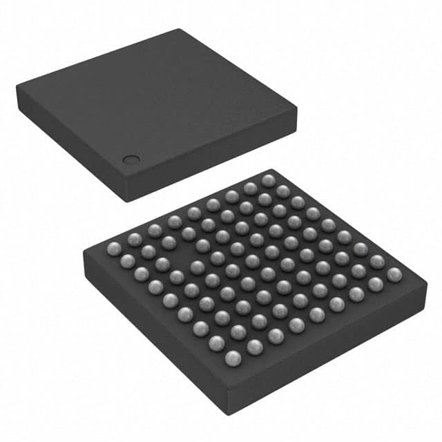
- Part No.:
- TUSB6015IZQER
- Manufacturer:
- Texas Instruments
- Category:
- Controllers
- Package:
- 80-VFBGA
- Datasheet:
-
 TUSB6015IZQER.pdf
- Description:
- IC USB 2.0 HS PERIPH CTRLR 80BGA
- Quantity:
- Payment:

- Shipping:

Inventory:4,964
Please send an inquiry. Send us your inquiry, and we will respond immediately.
Product details
Overview
TUSB6015IZQER from Texas Instruments is a USB 2.0 High-Speed (480 Mbps) peripheral controller IC with integrated PHY, NOR Flash–like 16/32-bit multiplexed host interface, six configurable endpoints (1 KB each), and eight GPIOs supporting DMA request and interrupt functions. It operates across industrial temperature (−40°C to +85°C) with dual supply domains (1.5 V core, 1.8 V I/O, 3.3 V analog) and supports CEA-936-A detection via DP/DM state-change interrupt.
For engineers reviewing the TUSB6015IZQER datasheet, TUSB6015IZQER pinout, TUSB6015IZQER application, or TUSB6015IZQER equivalent, this device serves as a low-power, BGA-packaged USB peripheral bridge for embedded host processors requiring high-speed data transfer, synchronous burst DMA access, and robust USB charging compliance up to 6 V VBUS.
Technical Context
The TUSB6015IZQER implements a full-speed and high-speed USB 2.0 transceiver with integrated 40.5–49.5 Ω HS driver termination, 100–150 mV squelch threshold, and ±1.3 µA DP/DM input leakage in idle mode. Its NOR Flash–like interface supports asynchronous single-access (16-/32-bit) and synchronous burst modes (16×16, DMA-enabled) at up to 65 MHz GPMC clock.
Power sequencing is controlled by active-low RSTn, with clock source selection latched on GPIO6 and CLK_24_SEL during reset; supported reference clocks are 19.2 MHz (square wave) or 38.4 MHz (sinusoid), both with ±100 ppm accuracy and sub-120 ps jitter. The device features failsafe LVCMOS I/Os that tolerate toggling without VDD18 applied.
Key Specifications
| Parameter | Value and Actual Design Meaning |
|---|---|
| USB Speed | USB 2.0 High-Speed compliant at 480 Mbps ±0.05%, meeting USB-IF TID #40630005 |
| Endpoint Count | Six physical endpoints, each independently configurable as IN or OUT with dedicated 1 KB FIFO buffer |
| Host Interface | NOR Flash–like 16-bit multiplexed address/data bus with asynchronous and synchronous burst (DMA) modes |
| Supply Voltages | VDD15 = 1.35–1.65 V (core), VDD18 = 1.62–1.98 V (I/O), VDDA3P3 = 3.0–3.6 V (PHY analog) |
| Operating Temperature | Industrial grade: −40°C to +85°C ambient, qualified per JEDEC JESD22-A104 |
| Package | 80-terminal BGA MICROSTAR JUNIOR (ZQE), RoHS-compliant, MSL Level-3 (260°C, 168 hr) |
| ESD Protection | 2 kV HBM (JESD22-A114D), 500 V CDM (JESD22-C101C) |
Pinout & Package
80-ball BGA MICROSTAR JUNIOR package (ZQE), 10 × 10 mm body, 0.5 mm pitch, bottom-side thermal pad. Requires precision external 10.7 kΩ ±1% resistor on R1 pin for PHY current calibration.
| Pin/Terminal | Circuit Role | Design Meaning |
|---|---|---|
| RSTn | Active-low system reset input | Latches clock configuration (GPIO6, CLK_24_SEL); holds internal core reset for 16 system clock cycles after deassertion |
| DP / DM | Differential USB 2.0 data pair | High-impedance when unpowered; support HS squelch detection (100–150 mV), chirp K/J signaling, and CEA-936-A state-change interrupt |
| ACSn / SCSn | Asynchronous / Synchronous chip select | Enable NOR-like interface access modes; SCSn synchronizes burst reads/writes to system clock (max 65 MHz) |
| ADVn / OEn / WEn | Address valid, output enable, write enable | Control multiplexed ADAT[0:16] bus timing; ADVn defines address setup/hold windows per TI timing specs |
| DMAREQ0–5 | DMA request outputs | Five dedicated DMA request signals (J7, J5, C4, E7, E8) tied to endpoint/FIFO activity for host-driven burst transfers |
| INT | Interrupt output | Open-drain signal asserted on DevReady, endpoint events, or DP/DM state change per CEA-936-A |
Key Features
| Feature | Design Value |
|---|---|
| Integrated USB 2.0 PHY | Meets USB-IF electrical compliance including HS driver output resistance (40.5–49.5 Ω), rise/fall time (≤500 ps), and VBUS tolerance up to 6 V |
| NOR Flash–like Host Interface | Supports 16-bit async, 32-bit async, and 16×16 sync burst with DMA - enabling zero-wait-state transfers at 65 MHz GPMC clock |
| Configurable GPIOs | Eight LVCMOS I/Os (GPIO0–7), each programmable as interrupt/wakeup source or secondary DMA request (GPIO1–5) |
| Power Sequencing Control | Failsafe I/O operation without VDD18; precise reset timing (≥3.3 µs pulse) ensures reliable clock source latching and PRCM initialization |
| Industrial Temperature Range | Qualified from −40°C to +85°C with supply voltage derating per spec: VDD15 min 1.35 V, VDD18 min 1.62 V |
Applications
| USB Peripheral Bridge for Industrial HMIs | Embedded Device Charging Controller |
|---|---|
Use Scenario: Human-machine interface (HMI) panel with ARM-based host processor requires high-bandwidth USB peripheral connectivity to PC host for firmware updates and real-time diagnostics. IC Role / Device Role / Timing Role: TUSB6015IZQER acts as USB 2.0 HS peripheral controller, interfacing host's NOR-like bus to USB cable; provides DevReady interrupt and endpoint FIFO management. Use Value: Enables 480 Mbps bulk transfers using synchronous burst DMA, reducing host CPU load and supporting deterministic update latency under industrial temperature stress. |
Use Scenario: Portable medical sensor hub must detect USB host presence, negotiate charging current, and maintain communication while drawing power from VBUS. IC Role / Device Role / Timing Role: TUSB6015IZQER monitors DP/DM state changes to trigger CEA-936-A detection interrupt and tolerates 6 V VBUS continuously for USB Battery Charging v1.2 compliance. Use Value: Eliminates need for external charger-detection IC; integrated PHY and failsafe I/O allow safe operation during partial power-up sequences common in battery-backed systems. |
| Legacy NOR Flash Replacement Interface | Low-Power USB Peripheral for Remote Sensors |
Use Scenario: Legacy industrial controller uses NOR Flash memory interface but requires USB connectivity for field service; redesign must retain same PCB footprint and bus timing. IC Role / Device Role / Timing Role: TUSB6015IZQER emulates NOR Flash timing (t_acsnl_advn_s = 18 ns, t_advn = 7 ns) while translating to USB protocol, accessed via identical address/data bus. Use Value: Enables drop-in replacement of legacy storage interface with USB peripheral functionality without modifying host software or PCB layout. |
Use Scenario: Wireless environmental sensor node powered by coin cell enters deep sleep between readings, waking only to transmit data over USB when host is connected. IC Role / Device Role / Timing Role: TUSB6015IZQER provides GPIO wakeup capability, ultra-low idle current (16.5 µA on VDDA3P3, 0.26 µA on VDD18), and DevReady signaling to synchronize host enumeration. Use Value: Achieves <1 µA system standby current with USB detect active, extending battery life beyond 5 years while maintaining full USB 2.0 HS compatibility. |
Equivalent & Alternatives
The following parts are listed as comparable options for similar USB 2.0 peripheral controller applications.
| Alternative Part | Technical Difference | Application Difference | Selection Advice |
|---|---|---|---|
| ISP1583B | PCI interface instead of NOR Flash–like; no integrated PHY (requires external UTMI+); 3.3 V only supply | Requires host PCI slot and external PHY; lacks CEA-936-A detection and VBUS 6 V tolerance | Select only if existing design uses PCI bus and external PHY layout is acceptable |
| USB334x series | USB 2.0 OTG controller with ULPI interface; supports host/peripheral dual-role; lower pin count (48-QFN) | Designed for portable devices with battery charging and OTG switching; no NOR Flash emulation or synchronous burst DMA | Prefer for space-constrained, dual-role applications where NOR interface compatibility is not required |
Compared with ISP1583B and USB334x, the TUSB6015IZQER uniquely delivers NOR Flash–like timing compatibility, integrated high-speed PHY with 6 V VBUS rating, and synchronous burst DMA-making it optimal for industrial host processors lacking PCI or ULPI interfaces but requiring seamless USB peripheral integration.
Availability
TUSB6015IZQER is available at Aetrix Electronics and suitable for industrial HMIs, USB charging controllers, legacy NOR Flash interface replacements, and low-power remote sensor peripherals requiring stable component supply and long-term lifecycle support.
Supply support for TUSB6015IZQER includes scheduled delivery planning, volume procurement assistance, BOM continuity management, traceable sourcing, and lifecycle availability coordination for OEM customers, industrial embedded developers, connected-device designers, and electronics production programs.
Manufacturer
Texas Instruments is a global semiconductor company headquartered in Dallas, Texas, delivering analog and embedded processing solutions for industrial, automotive, and communications markets since 1930.
The TUSB6015IZQER belongs to TI's USB peripheral controller product line, designed specifically to simplify USB 2.0 HS integration for resource-constrained host processors using standard memory-mapped interfaces-targeting industrial control, medical devices, and test equipment.
FAQ
What USB speed modes does the TUSB6015IZQER support?
The TUSB6015IZQER supports full-speed (12 Mbps) and high-speed (480 Mbps) USB 2.0 modes. It automatically negotiates high-speed upon connection if the host supports it, using built-in chirp K/J signaling and squelch detection (100–150 mV differential threshold). The device is USB-IF certified (TID #40630005) and meets all electrical compliance requirements for both modes.
Does the TUSB6015IZQER require an external crystal or oscillator?
No, the TUSB6015IZQER does not require an external crystal. It accepts either a 19.2 MHz square-wave clock (via CLKIN_19_2_24) or a 38.4 MHz sinusoidal clock (via CLKIN_38_4), selected at reset using GPIO6 and CLK_24_SEL pins. Clock accuracy must be ±100 ppm, with jitter ≤118 ps peak-to-peak for reliable USB 2.0 HS operation.
How many endpoints does the TUSB6015IZQER provide, and how are they configured?
The TUSB6015IZQER provides six physical endpoints, each configurable as IN or OUT direction via host software. Each endpoint has a dedicated 1 KB buffer, and endpoint types (control, bulk, interrupt, isochronous) are defined in descriptor tables loaded by the host. Configuration is performed through the NOR Flash–like interface during enumeration.
What is the purpose of the R1 pin on the TUSB6015IZQER?
The R1 pin connects to a precision 10.7 kΩ ±1% external resistor that calibrates internal reference currents for the USB 2.0 PHY, ensuring accurate driver output impedance (40.5–49.5 Ω), current levels, and compliance with USB 2.0 specification requirements. This resistor must be placed close to the R1 ball with low-inductance ground return.
Is the TUSB6015IZQER compatible with modern USB-C or USB Power Delivery?
The TUSB6015IZQER is a USB 2.0 peripheral controller and does not implement USB-C connector logic or USB Power Delivery (USB-PD) protocol. It supports USB Battery Charging v1.2 via its 6 V VBUS tolerance and CEA-936-A detection, but requires external circuitry (e.g., CC logic IC) for full USB-C or USB-PD functionality.
TUSB6015IZQER Specifications
- Product attributes
- Attribute value
- Manufacturer:
- Texas Instruments
- Package/Case:
- 80-VFBGA
- Programmable:
- Not Verified
- Protocol:
- USB
- Function:
- Controller
- Interface:
- USB
- Standards:
- USB 2.0
- Voltage - Supply:
- 3V ~ 3.6V
- Current - Supply:
- -
- Operating Temperature:
- -40°C ~ 85°C
- Supplier Device Package:
- 80-BGA MICROSTAR JUNIOR (5x5)
- Grade:
- -
- Qualification:
- -
TUSB6015IZQER FAQ
1.How can I place an order for TUSB6015IZQER through Aetrix?
Please submit a Request for Quotation (RFQ) for TUSB6015IZQER on Aetrix. Our sales agent will provide a competitive quotation and guide you through the order confirmation once you accept the terms.
2.Are the price and stock information for TUSB6015IZQER reliable?
The price and inventory of TUSB6015IZQER are updated periodically and may fluctuate due to market conditions. Stock and pricing data are typically refreshed every 24 hours. Quotation validity for TUSB6015IZQER is usually 5 days.
3.What payment methods are accepted for TUSB6015IZQER?
We accept Wire Transfer, PayPal, Credit Card, Western Union, MoneyGram, and Escrow for TUSB6015IZQER transactions.
Note: Certain payment methods may incur a processing fee.
4.How is shipping managed for TUSB6015IZQER?
TUSB6015IZQER orders can be shipped via leading logistics carriers, including DHL, UPS, FedEx, TNT, or Registered Mail.
Once your TUSB6015IZQER order is processed, you will receive an email with the shipment details and tracking number.
Note: Tracking information may take up to 24 hours to appear. Express delivery typically takes 3–5 business days.
5.How can I obtain technical support or documentation for TUSB6015IZQER?
For technical support, including TUSB6015IZQER datasheets, pinout diagrams, or application guidance, please contact our engineering support team. They can provide detailed documentation and assistance for your TUSB6015IZQER requirements.
6.How does Aetrix verify that TUSB6015IZQER is sourced from the original manufacturer or authorized distributors?
All TUSB6015IZQER products on Aetrix are procured from qualified distributors and authorized channels. Our dedicated quality assurance team conducts strict verification, including traceability checks and, if necessary, third-party testing. This ensures that TUSB6015IZQER meets industry standards.
7.What is the process for return or replacement of TUSB6015IZQER?
All TUSB6015IZQER units undergo pre-shipment inspection (PSI). If there is an issue with TUSB6015IZQER, returns or replacements are accepted under the following conditions:
1.Quantity discrepancies, incorrect items, or visible external defects (such as breakage or corrosion), acknowledged by Aetrix.
2.The issue is reported within 90 days of delivery.
3.The TUSB6015IZQER part is unused and in its original packaging.
Return procedure for TUSB6015IZQER:
1.Submit a request within 90 days.
2.Obtain a Return Material Authorization (RMA) from Aetrix.
TUSB6015IZQER Tags

-
PTN5150AHXMP
NXP Semiconductors

-
USB3740B-AI9-TR
Microchip Technology

-
USB3740B-AI2-TR
Microchip Technology

-
USB3300-EZK-TR
Microchip Technology
-
USB3300-EZK
Microchip Technology

-
FUSB340TMX
onsemi

-
FUSB302BMPX
onsemi

-
DP83826IRHBR
Texas Instruments

-
MCP2518FDT-E/QBB
Microchip Technology
-
FUSB302MPX
onsemi

-
MCP2518FDT-E/SL
Microchip Technology

-
FT260Q-R
FTDI, Future Technology Devices International Ltd
Tech Hub

A practical engineering guide to 3.3V and 5V logic compatibility, input thresholds, resistor dividers, translator ICs, MOSFET level shifting, I2C pull-ups, timing limits and power-sequencing risks.

The 74HC595 uses push-pull logic outputs, while the TPIC6B595 uses 50 V open-drain DMOS sinks for higher-power loads. This guide compares timing, current limits, 3.3 V interfacing, load wiring, thermal…

The 74HC595 converts serial data into eight stable parallel outputs. This guide covers pin functions, shift and storage timing, OE and MR behavior, drive-current limits, cascading, voltage compatibilit…

A technical comparison of level-sensitive latches and edge-triggered flip-flops, covering timing windows, setup and hold limits, master–slave operation, time borrowing, race-through, HDL inference and…

A D latch stores one bit while Enable controls when data can pass. This reference covers gate-level operation, truth tables, transparency, setup and hold timing, LE versus OE, common ICs and practical …

An SR latch stores one bit through cross-coupled feedback. This engineering reference covers NOR and NAND implementations, truth tables, forbidden-state recovery, gated operation, switch debouncing, fa…

Latch circuits retain one bit through feedback. This technical reference covers SR and D latches, truth tables, transparency, timing limits, latch-versus-flip-flop behavior, applications and common log…

An engineering guide to LED driver operation, constant-current and constant-voltage outputs, linear and switching topologies, dimming, IC selection, calculations, replacement compatibility, and fault c…

Operational amplifier guide covering op amp basics, feedback, ideal vs real op amps, common configurations, buffer circuits, offset, bias current, gain-bandwidth, slew rate, rail-to-rail limits and sel…

Jumper cables guide covering safe connection order, red and black clamp placement, final ground connection, cable gauge, length, clamp quality, copper vs CCA cables, jump starter comparison and battery…


