
 My Inquiry
 My Account


Texas Instruments TUSB8042RGCR
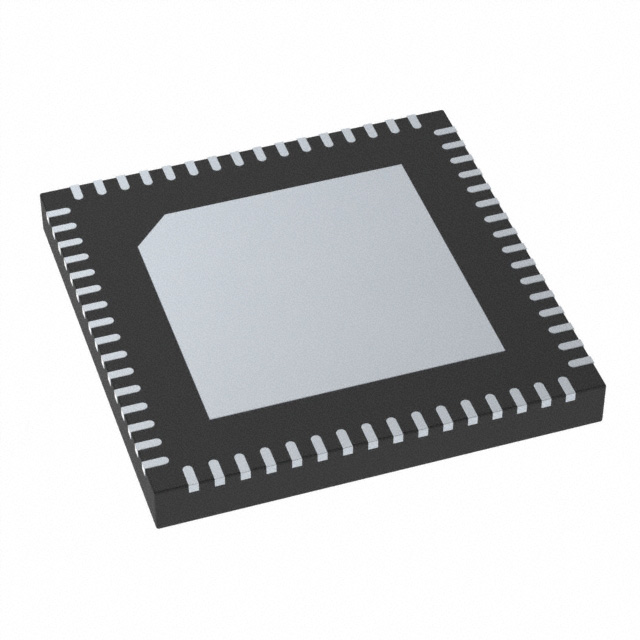
- Part No.:
- TUSB8042RGCR
- Manufacturer:
- Texas Instruments
- Category:
- Controllers
- Package:
- 64-VFQFN Exposed Pad
- Datasheet:
-
 TUSB8042RGCR.pdf
- Description:
- IC USB HUB CNTRLR 64VQFN
- Quantity:
- Payment:

- Shipping:

Inventory:1,403
Please send an inquiry. Send us your inquiry, and we will respond immediately.
Product details
Overview
TUSB8042RGCR from Texas Instruments is a four-port USB 3.1 Gen1 hub IC supporting simultaneous SuperSpeed (5 Gbps) and high-speed (480 Mbps) upstream connectivity, with per-port configurable downstream support for SuperSpeed, high-speed, full-speed, or low-speed USB devices; operates across 0°C to 70°C and integrates MTT architecture with four transaction translators for concurrent USB 2.0 traffic handling - deployed in docking stations and monitors requiring robust multi-speed USB expansion.
For engineers reviewing the TUSB8042RGCR datasheet, TUSB8042RGCR pinout, TUSB8042RGCR application, or TUSB8042RGCR equivalent, key selection criteria include its 64-pin VQFN (RGC) package, dual-supply operation (1.1 V / 3.3 V), battery charging support (CDP/DCP/ACP modes), I²C/SMBus configurability, and USB 3.1 Gen1 compliance with backward compatibility to USB 2.0/1.1.
Technical Context
The TUSB8042RGCR implements a Multi-Transaction Translator (MTT) hub architecture with four independent transaction translators and two asynchronous endpoint buffers per translator, enabling concurrent high-bandwidth USB 2.0 device communication without bandwidth contention. It supports dynamic upstream link negotiation: SuperSpeed is disabled on downstream ports when upstream connects only to high-speed or full-speed environments.
Its power management includes per-port or ganged PWRCTL/BATEN control with OVERCURz detection inputs, and battery charging logic compliant with USB BC1.2, YD/T 1591-2009, and Galaxy Charging protocols. Configuration is supported via pin strapping, OTP ROM, or external I²C EEPROM at 100 kHz/400 kHz.
Key Specifications
| Parameter | Value and Actual Design Meaning |
|---|---|
| USB Standard | USB 3.1 Gen1 (5 Gbps) + USB 2.0 (480 Mbps) compliant hub with full backward compatibility to USB 1.1 |
| Port Count | Four downstream ports + one upstream port; all downstream ports independently configurable for SS/HS/FS/LS |
| Supply Voltages | 1.1 V (VDD) core rail and 3.3 V (VDD33) I/O rail; specified operating range: 0.99–1.26 V and 3.0–3.6 V respectively |
| Operating Temperature | 0°C to 70°C ambient; junction temperature rated up to 105°C with RθJA = 26°C/W in 64-pin VQFN package |
| Battery Charging Modes | Supports CDP (upstream connected), DCP (upstream unconnected, YD/T 1591-2009 compliant), and ACP1–ACP3 divider modes with automatic transition |
| Configuration Interface | I²C/SMBus slave interface (100/400 kHz), OTP ROM, or serial EEPROM for VID/PID, port customization, and string storage |
| ESD Rating | ±2000 V HBM per ANSI/ESDA/JEDEC JS-001; ±500 V CDM per JESD22-C101 |
Pinout & Package
Package: 64-pin VQFN (RGC), 9.00 mm × 9.00 mm body size with exposed thermal pad (VSS) requiring PCB ground connection.
| Pin/Terminal | Circuit Role | Design Meaning |
|---|---|---|
| USB_SSTXP_UP / USB_SSTXM_UP | Upstream SuperSpeed differential transmitter | Drives 5-Gbps differential signaling to host controller; requires controlled 90-Ω impedance routing |
| USB_SSRXP_UP / USB_SSRXM_UP | Upstream SuperSpeed differential receiver | Receives 5-Gbps differential signals from host; AC-coupled with 100-nF capacitors per TI layout guidelines |
| PWRCTL1–PWRCTL4 / BATEN1–BATEN4 | Per-port power control & battery enable | Active-high or active-low (configurable via PWRCTL_POL) outputs to drive external load switches for downstream port power gating |
| OVERCUR1z–OVERCUR4z | Per-port over-current detection input | Active-low open-drain inputs monitoring external current-limiting switch status; asserted during fault condition |
| SCL/SMBCLK & SDA/SMBDAT | I²C/SMBus configuration interface | Configurable via SMBUSz pin; supports EEPROM programming of VID/PID, port settings, and manufacturer strings |
| GRSTz | Global reset input | Active-low asynchronous reset; must be held low ≥3 ms after both VDD and VDD33 stabilize before de-assertion |
Key Features
| Feature | Design Value |
|---|---|
| Multi-Transaction Translator (MTT) | Four independent TTs with two async endpoint buffers each eliminate USB 2.0 bandwidth bottlenecks across multiple downstream devices |
| Flexible Power Management | Per-port or ganged PWRCTL control with dedicated OVERCURz inputs enables selective port shutdown during faults without affecting other ports |
| USB Battery Charging Support | Hardware-accelerated CDP, DCP (YD/T 1591-2009), and ACP mode handshaking - no host software intervention required for charger detection |
| Configurability Options | Pin-strapped defaults, OTP ROM, or external I²C EEPROM allow field-programmable VID/PID, port enable/disable, and PHY tuning |
| Single-Crystal Clock Input | 24-MHz crystal or oscillator on XI/XO pins eliminates need for external clock generator; internal PLL generates required USB timing domains |
Applications
| Docking Stations | Monitors with USB Hub |
|---|---|
|
Use Scenario: Desktop docking station aggregating keyboard, mouse, storage, and display peripherals via single USB-C upstream connection. IC Role / Device Role / Timing Role: USB 3.1 Gen1 hub managing concurrent SuperSpeed SSD traffic and high-speed HID data while maintaining precise USB packet timing alignment. Use Value: Enables full-bandwidth peripheral connectivity without USB 2.0 transaction translator contention, reducing latency for time-sensitive HID and audio endpoints. |
Use Scenario: Smart monitor with integrated USB hub providing downstream ports for webcam, headset, and flash drive alongside video input. IC Role / Device Role / Timing Role: Four-port hub IC handling mixed-speed downstream devices while synchronizing suspend/resume states with upstream host via SS_SUSPEND and HS_SUSPEND signals. Use Value: Delivers reliable battery charging (CDP/DCP) to connected mobile devices without requiring host OS driver modifications. |
| Set-Top Boxes | Industrial Control Panels |
|
Use Scenario: Media streaming box with front-panel USB ports for firmware updates, external storage, and IR receivers. IC Role / Device Role / Timing Role: USB 2.0/3.1 bridge IC providing isolated downstream port power control and over-current protection per port. Use Value: Prevents system-wide failure during short-circuit events on one port by disabling only the affected downstream power path. |
Use Scenario: Factory HMI panel connecting barcode scanners, USB printers, and configuration dongles in harsh ESD-prone environments. IC Role / Device Role / Timing Role: Robust USB hub IC with ±2000-V HBM ESD rating and 0°C–70°C commercial temp grade ensuring long-term reliability in industrial enclosures. Use Value: Eliminates need for external ESD protection components on downstream ports due to integrated high-threshold I/O structures. |
Equivalent & Alternatives
The following parts are listed as comparable options for similar USB 3.1 Gen1 hub applications.
| Alternative Part | Technical Difference | Application Difference | Selection Advice |
|---|---|---|---|
| USB3503A-AEZG | Three-port USB 3.0 hub with integrated USB 2.0 PHY; lacks MTT architecture and battery charging hardware acceleration | Lower port count and no native DCP/ACP support; requires external charging IC or host-based BC1.2 negotiation | Preferred where compact 48-QFN footprint and lower BOM cost outweigh need for four ports or hardware charging |
| TUSB8041RGCR | Pin-compatible 4-port variant with identical RGC package but lacks I²C/SMBus slave interface and OTP ROM; fixed VID/PID only | No field-updatable configuration; limited to factory-programmed settings - unsuitable for OEM branding or multi-product reuse | Select when configuration flexibility is unnecessary and cost reduction via simplified firmware provisioning is prioritized |
Compared with USB3503A-AEZG and TUSB8041RGCR, the TUSB8042RGCR uniquely delivers four-port MTT performance, hardware-enforced battery charging modes, and full I²C/SMBus configurability - making it optimal for docking stations and branded peripherals requiring differentiated feature sets and field programmability.
Availability
TUSB8042RGCR is available at Aetrix Electronics and suitable for docking stations, monitors, set-top boxes, and industrial control panels requiring stable component supply, long-lifecycle availability, and consistent USB 3.1 Gen1 compliance across production batches.
Supply support for TUSB8042RGCR includes scheduled delivery planning, volume procurement assistance, BOM continuity management, traceable sourcing, and lifecycle availability coordination for OEM customers, industrial embedded developers, connected-device designers, and electronics production programs.
Manufacturer
Texas Instruments is a global semiconductor company specializing in analog, embedded processing, and connectivity technologies, with decades of leadership in USB interface solutions and industrial-grade IC design.
The TUSB8042RGCR belongs to TI's USB 3.x hub product line, engineered specifically for high-reliability, multi-speed peripheral aggregation in space-constrained consumer and industrial systems requiring seamless USB 2.0/3.1 coexistence.
FAQ
What USB speed modes does the TUSB8042RGCR support on its downstream ports?
The TUSB8042RGCR supports SuperSpeed (5 Gbps), high-speed (480 Mbps), full-speed (12 Mbps), and low-speed (1.5 Mbps) on all four downstream ports. Downstream speed capability is dynamically determined by the upstream link: SuperSpeed is disabled if upstream connects only to high-speed or full-speed environments; both SuperSpeed and high-speed are disabled if upstream connects only to full-speed/low-speed environments. This behavior is hardware-managed and requires no firmware intervention.
Does the TUSB8042RGCR require an external crystal, and what are the clock requirements?
Yes, the TUSB8042RGCR requires a 24-MHz crystal connected between XI and XO pins, or a 24-MHz CMOS oscillator driving the XI pin. A 1-MΩ feedback resistor is mandatory between XI and XO when using a crystal. The internal PLL derives all required USB timing domains (e.g., 125 MHz for SuperSpeed, 48 MHz for USB 2.0) from this reference - no additional clock sources are needed for compliant operation.
How does battery charging work on the TUSB8042RGCR, and which standards are supported?
The TUSB8042RGCR implements hardware-based battery charging detection per USB Battery Charging Specification Rev 1.2. It supports Charging Downstream Port (CDP) mode when upstream is connected, Dedicated Charging Port (DCP) mode when upstream is unconnected (compliant with YD/T 1591-2009), and three Divider Charging Port (ACP1–ACP3) modes with automatic sequential transition. All modes operate without host CPU involvement, using dedicated BATENx and AUTOENz pins sampled at reset.
Can the TUSB8042RGCR be configured after manufacturing, and what interfaces are available?
Yes, the TUSB8042RGCR supports post-manufacturing configuration via I²C or SMBus interface (SCL/SMBCLK and SDA/SMBDAT pins), OTP ROM, or external serial EEPROM. Supported parameters include VID/PID, port enable/disable states, battery charging enable per port, manufacturer/product strings, and custom PHY settings. Pin strapping provides default configuration when external interfaces are unused.
What is the thermal performance of the TUSB8042RGCR in its 64-pin VQFN package?
The TUSB8042RGCR in the 64-pin VQFN (RGC) package has a junction-to-ambient thermal resistance (RθJA) of 26°C/W under standard JEDEC test conditions. Its junction-to-board (RθJB) is 5.3°C/W, indicating strong heat conduction through the PCB. Maximum operating junction temperature is 105°C, with recommended ambient operation from 0°C to 70°C - thermal design must ensure adequate copper area under the exposed VSS pad and proper airflow for sustained full-load operation.
TUSB8042RGCR Specifications
- Product attributes
- Attribute value
- Manufacturer:
- Texas Instruments
- Package/Case:
- 64-VFQFN Exposed Pad
- Programmable:
- Not Verified
- Protocol:
- USB
- Function:
- Hub Controller
- Interface:
- USB, GPIO, I2C, SMBus
- Standards:
- USB 3.0
- Voltage - Supply:
- 1.1V, 3.3V
- Current - Supply:
- -
- Operating Temperature:
- 0°C ~ 70°C
- Supplier Device Package:
- 64-VQFN (9x9)
- Grade:
- -
- Qualification:
- -
TUSB8042RGCR FAQ
1.How can I place an order for TUSB8042RGCR through Aetrix?
Please submit a Request for Quotation (RFQ) for TUSB8042RGCR on Aetrix. Our sales agent will provide a competitive quotation and guide you through the order confirmation once you accept the terms.
2.Are the price and stock information for TUSB8042RGCR reliable?
The price and inventory of TUSB8042RGCR are updated periodically and may fluctuate due to market conditions. Stock and pricing data are typically refreshed every 24 hours. Quotation validity for TUSB8042RGCR is usually 5 days.
3.What payment methods are accepted for TUSB8042RGCR?
We accept Wire Transfer, PayPal, Credit Card, Western Union, MoneyGram, and Escrow for TUSB8042RGCR transactions.
Note: Certain payment methods may incur a processing fee.
4.How is shipping managed for TUSB8042RGCR?
TUSB8042RGCR orders can be shipped via leading logistics carriers, including DHL, UPS, FedEx, TNT, or Registered Mail.
Once your TUSB8042RGCR order is processed, you will receive an email with the shipment details and tracking number.
Note: Tracking information may take up to 24 hours to appear. Express delivery typically takes 3–5 business days.
5.How can I obtain technical support or documentation for TUSB8042RGCR?
For technical support, including TUSB8042RGCR datasheets, pinout diagrams, or application guidance, please contact our engineering support team. They can provide detailed documentation and assistance for your TUSB8042RGCR requirements.
6.How does Aetrix verify that TUSB8042RGCR is sourced from the original manufacturer or authorized distributors?
All TUSB8042RGCR products on Aetrix are procured from qualified distributors and authorized channels. Our dedicated quality assurance team conducts strict verification, including traceability checks and, if necessary, third-party testing. This ensures that TUSB8042RGCR meets industry standards.
7.What is the process for return or replacement of TUSB8042RGCR?
All TUSB8042RGCR units undergo pre-shipment inspection (PSI). If there is an issue with TUSB8042RGCR, returns or replacements are accepted under the following conditions:
1.Quantity discrepancies, incorrect items, or visible external defects (such as breakage or corrosion), acknowledged by Aetrix.
2.The issue is reported within 90 days of delivery.
3.The TUSB8042RGCR part is unused and in its original packaging.
Return procedure for TUSB8042RGCR:
1.Submit a request within 90 days.
2.Obtain a Return Material Authorization (RMA) from Aetrix.
TUSB8042RGCR Tags

-
PTN5150AHXMP
NXP Semiconductors

-
USB3740B-AI9-TR
Microchip Technology

-
USB3740B-AI2-TR
Microchip Technology

-
USB3300-EZK-TR
Microchip Technology
-
USB3300-EZK
Microchip Technology

-
FUSB340TMX
onsemi

-
FUSB302BMPX
onsemi

-
DP83826IRHBR
Texas Instruments

-
MCP2518FDT-E/QBB
Microchip Technology
-
FUSB302MPX
onsemi

-
MCP2518FDT-E/SL
Microchip Technology

-
FT260Q-R
FTDI, Future Technology Devices International Ltd
Tech Hub

A practical engineering guide to 3.3V and 5V logic compatibility, input thresholds, resistor dividers, translator ICs, MOSFET level shifting, I2C pull-ups, timing limits and power-sequencing risks.

The 74HC595 uses push-pull logic outputs, while the TPIC6B595 uses 50 V open-drain DMOS sinks for higher-power loads. This guide compares timing, current limits, 3.3 V interfacing, load wiring, thermal…

The 74HC595 converts serial data into eight stable parallel outputs. This guide covers pin functions, shift and storage timing, OE and MR behavior, drive-current limits, cascading, voltage compatibilit…

A technical comparison of level-sensitive latches and edge-triggered flip-flops, covering timing windows, setup and hold limits, master–slave operation, time borrowing, race-through, HDL inference and…

A D latch stores one bit while Enable controls when data can pass. This reference covers gate-level operation, truth tables, transparency, setup and hold timing, LE versus OE, common ICs and practical …

An SR latch stores one bit through cross-coupled feedback. This engineering reference covers NOR and NAND implementations, truth tables, forbidden-state recovery, gated operation, switch debouncing, fa…

Latch circuits retain one bit through feedback. This technical reference covers SR and D latches, truth tables, transparency, timing limits, latch-versus-flip-flop behavior, applications and common log…

An engineering guide to LED driver operation, constant-current and constant-voltage outputs, linear and switching topologies, dimming, IC selection, calculations, replacement compatibility, and fault c…

Operational amplifier guide covering op amp basics, feedback, ideal vs real op amps, common configurations, buffer circuits, offset, bias current, gain-bandwidth, slew rate, rail-to-rail limits and sel…

Jumper cables guide covering safe connection order, red and black clamp placement, final ground connection, cable gauge, length, clamp quality, copper vs CCA cables, jump starter comparison and battery…


