
 My Inquiry
 My Account


Renesas TW9920-BC1-GR
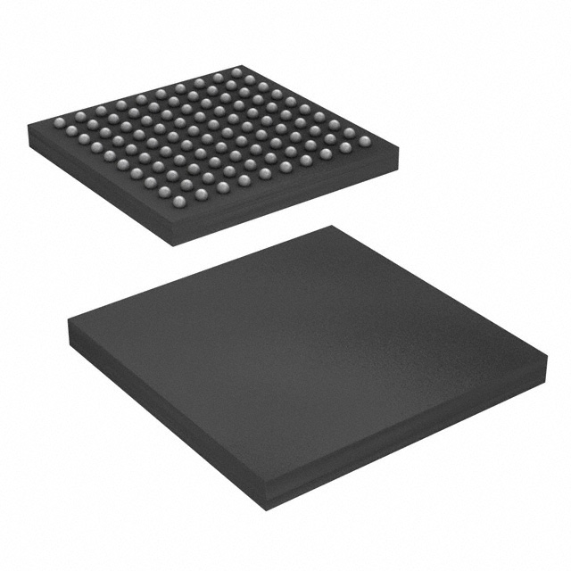
- Part No.:
- TW9920-BC1-GR
- Manufacturer:
- Renesas
- Category:
- Encoders, Decoders, Converters
- Package:
- 100-LBGA
- Datasheet:
-
 TW9920-BC1-GR.pdf
- Description:
- IC DECODER/ENCODER VIDEO 100BGA
- Quantity:
- Payment:

- Shipping:

Inventory:3,209
Please send an inquiry. Send us your inquiry, and we will respond immediately.
Product details
Overview
TW9920-BC1-GR from Intersil is a multistandard analog video decoder and encoder IC designed for embedded multimedia systems. It supports NTSC/PAL/SECAM decoding with 4H comb filtering, converts CVBS/S-Video to ITU-R 601/656 YCbCr(4:2:2), and encodes digital YCbCr back to analog CVBS or S-Video. Typical power consumption is 0.62W at 2.5/3.3V supply.
For engineers reviewing the TW9920-BC1-GR datasheet, TW9920-BC1-GR pinout, TW9920-BC1-GR application, or TW9920-BC1-GR equivalent, key selection considerations include multistandard auto-detection, integrated 4H comb filter performance, VBI slicer capability, dual-direction YCbCr interface compliance, and VFBGA-80 package constraints.
Technical Context
The TW9920-BC1-GR integrates independent decoder and encoder signal chains sharing a single 27MHz crystal reference. Its decoder employs dual 9-bit ADCs with analog clamping, digital horizontal PLL for pixel sampling, and adaptive 4H comb filter for Y/C separation - enabling robust NTSC/PAL/SECAM handling under weak or nonstandard sync conditions.
The encoder uses five 10-bit DACs operating at 27MHz to simultaneously generate CVBS, Y/C, and YCbCr outputs. It includes luminance/chrominance filtering, field-locked audio clock generation, and supports ITU-R 656 input timing - all while maintaining sub-1/32-pixel horizontal phase accuracy during scaling.
Key Specifications
| Parameter | Value and Actual Design Meaning |
|---|---|
| Video Standards | NTSC (M, 4.43), PAL (B/D/G/H/I/M/N/N-comb), PAL(60), SECAM with automatic format detection |
| ADC Resolution | Dual 9-bit ADCs with analog clamping for CVBS/S-Video inputs |
| DAC Resolution | Five 10-bit DACs at 27MHz sample rate for simultaneous CVBS/Y/C/YCbCr output |
| Output Format | ITU-R 601/656 compliant YCbCr(4:2:2) digital output; supports cropping & VBI data pass-through |
| Power Supply | 2.5V or 3.3V core; 3V-tolerant I/O; typical power draw 0.62W |
| Clock Source | Single 27MHz crystal for all standards; also supports 24.54MHz/29.5MHz for square-pixel high-res decoding |
| Interface | Two-wire MPU serial bus (I²C-compatible) for register configuration and control |
Pinout & Package
VFBGA-80 package (5mm × 5mm, 0.5mm pitch), ball-grid array with defined power, ground, analog input, digital I/O, and crystal connections.
| Pin/Terminal | Circuit Role | Design Meaning |
|---|---|---|
| AVDD/AVSS | Analog power/ground | Separate 2.5/3.3V analog supply domain for ADC/DAC blocks; requires local decoupling |
| DVDD/DVSS | Digital power/ground | Dedicated 2.5/3.3V digital supply for logic, PLLs, and interface; isolated from analog domains |
| CVBS_IN0–3 / Y_IN0–3 / C_IN0–3 | Analog video inputs | Configurable as up to four CVBS or three CVBS + one Y/C pair; software-selectable routing |
| YOUT[7:0], COUT[7:0], YCOUT[7:0] | Digital YCbCr output buses | 8-bit parallel ITU-R 601/656 Y/C or multiplexed YCbCr(4:2:2) output with embedded sync |
| SCL/SDA | MPU interface | I²C-compatible two-wire serial bus for register read/write; supports standard/fast mode |
| XIN/XOUT | Clock oscillator terminals | Connects to external 27MHz (or 24.54/29.5MHz) crystal; internal oscillator circuitry drives all PLLs |
Key Features
| Feature | Design Value |
|---|---|
| 4-H adaptive comb filter | Reduces cross-luminance and cross-color artifacts in NTSC/PAL decoding without requiring external delay lines |
| Digital subcarrier PLL | Enables precise color burst locking across NTSC/PAL/SECAM standards, improving hue stability under signal drift |
| VBI slicer with Intercast™ support | Extracts closed captioning, teletext, and industrial data services directly from raw ADC output |
| Programmable image enhancement | Independent 2D peaking, CTI, gamma, noise suppression, and color controls allow real-time tuning per system requirement |
| Field-locked audio clock | Generates stable audio sampling clocks synchronized to video field rate, eliminating lip-sync drift in AV systems |
Applications
| Automotive Rear-View Camera Systems | Industrial Video Surveillance DVRs |
|---|---|
Use Scenario: Analog camera feeds (CVBS) from backup cameras are digitized and processed before display on infotainment screens. IC Role / Device Role / Timing Role: TW9920-BC1-GR acts as the primary video front-end, performing NTSC decoding, Y/C separation, and ITU-R 656 formatting for SoC ingestion. Use Value: Integrated 4H comb filter and automatic standard detection eliminate manual configuration and improve image clarity in variable lighting conditions. | Use Scenario: Legacy analog CCTV cameras feed multiple CVBS streams into a multi-channel DVR for compression and storage. IC Role / Device Role / Timing Role: TW9920-BC1-GR serves as a channelized decoder with VBI data extraction for time-stamping and metadata embedding. Use Value: Simultaneous cropping, VBI slicing, and programmable gain control enable per-channel optimization without external logic. |
| Medical Endoscopy Display Units | Legacy Broadcast Equipment Upgrades |
Use Scenario: High-reliability analog video from endoscopic probes must be converted to digital for real-time display and recording. IC Role / Device Role / Timing Role: TW9920-BC1-GR provides low-latency, artifact-free decoding with configurable sharpness and noise suppression for diagnostic clarity. Use Value: 2D peaking and CTI enhancement preserve edge fidelity critical for tissue differentiation, while 0.62W power enables fanless enclosure design. | Use Scenario: Retrofitting aging broadcast monitors or test equipment to accept modern digital video sources via analog output conversion. IC Role / Device Role / Timing Role: TW9920-BC1-GR functions as a precision encoder, converting ITU-R 656 YCbCr to broadcast-compliant CVBS/S-Video with calibrated luminance/chrominance filtering. Use Value: Five 10-bit DACs and stable 27MHz subcarrier generation ensure broadcast-grade color fidelity and sync stability. |
Equivalent & Alternatives
The following parts are listed as comparable options for similar analog video decoder/encoder applications.
| Alternative Part | Technical Difference | Application Difference | Selection Advice |
|---|---|---|---|
| ADV7180BCPZ | Single-function decoder only (no encoder); 10-bit ADC; supports NTSC/PAL but no SECAM or VBI slicer | Limited to decode-only systems requiring lower BOM count; lacks dual-direction functionality | Select when encoder functionality is unnecessary and SECAM/VBI support is not required |
| THS8200IPFP | Encoder-only device; 10-bit DACs; supports RGB/YCbCr-to-CVBS/S-Video; no decoder or comb filter | Used in digital-source-to-analog-output paths only; cannot process analog camera inputs | Choose when system already digitizes video upstream and only analog output generation is needed |
Compared with ADV7180BCPZ and THS8200IPFP, the TW9920-BC1-GR uniquely combines full multistandard decode + encode in one VFBGA-80 package, enabling bidirectional analog/digital video bridging without external buffering or dual-chip layout complexity.
Availability
TW9920-BC1-GR is available at Aetrix Electronics and suitable for automotive rear-view camera systems, industrial DVRs, medical endoscopy displays, and broadcast equipment upgrades requiring stable component supply and long-term manufacturability.
Supply support for TW9920-BC1-GR includes scheduled delivery planning, volume procurement assistance, BOM continuity management, traceable sourcing, and lifecycle availability coordination for OEM customers, industrial embedded developers, connected-device designers, and electronics production programs.
Manufacturer
Intersil Corporation, now part of Renesas Electronics, designs high-performance analog and mixed-signal ICs for power management, precision analog, and video infrastructure applications.
The TW9920-BC1-GR belongs to Intersil's legacy video processing product line, engineered specifically for cost-sensitive, space-constrained embedded systems needing seamless analog-to-digital and digital-to-analog video translation.
FAQ
What video standards does the TW9920-BC1-GR support?
The TW9920-BC1-GR supports NTSC (M, 4.43), PAL (B, D, G, H, I, M, N, N-comb), PAL(60), and SECAM with automatic format detection. It uses digital PLLs and adaptive filtering to maintain accurate color decoding and synchronization across all standards without manual intervention. The TW9920-BC1-GR achieves this using a single 27MHz crystal and integrated subcarrier generation circuitry.
Does the TW9920-BC1-GR include both decoder and encoder functionality?
Yes, the TW9920-BC1-GR integrates a full multistandard analog video decoder and a high-fidelity digital video encoder in a single IC. It decodes CVBS or S-Video into ITU-R 601/656 YCbCr(4:2:2), and encodes digital YCbCr back to CVBS or S-Video using five 10-bit DACs. This dual functionality eliminates the need for separate decoder and encoder chips in bidirectional video systems like the TW9920-BC1-GR.
What is the package type and pin count of the TW9920-BC1-GR?
The TW9920-BC1-GR uses a VFBGA-80 package measuring 5mm × 5mm with 0.5mm ball pitch. It contains 80 solder balls arranged in a grid, including dedicated analog power/ground, digital I/O, video input/output, and crystal interface connections. The TW9920-BC1-GR's VFBGA footprint requires controlled-depth reflow and microvia PCB design for reliable assembly.
Can the TW9920-BC1-GR handle VBI data extraction?
Yes, the TW9920-BC1-GR includes an integrated VBI slicer supporting closed captioning, teletext, and industrial data services. It allows raw ADC data pass-through for Intercast™ compatibility and enables direct extraction of timing-critical metadata without external processors. This VBI capability is fully functional across all supported standards and is configurable via the TW9920-BC1-GR's I²C interface.
What power supply requirements does the TW9920-BC1-GR have?
The TW9920-BC1-GR operates from separate 2.5V or 3.3V analog (AVDD) and digital (DVDD) supplies, with 3V-tolerant I/O. Its typical power consumption is 0.62W under full operation. Decoupling capacitors must be placed near AVDD/AVSS and DVDD/DVSS pins to maintain signal integrity. The TW9920-BC1-GR's low-power architecture supports fanless thermal design in compact enclosures.
TW9920-BC1-GR Specifications
- Product attributes
- Attribute value
- Manufacturer:
- Renesas
- Series:
- -
- Package/Case:
- 100-LBGA
- Packaging:
- Tray
- Product Status:
- Obsolete
- Type:
- Video Decoder, Encoder
- Applications:
- Cell Phone
- Voltage - Supply, Analog:
- 2.5V, 3.3V
- Voltage - Supply, Digital:
- 2.5V, 3.3V
- Grade:
- -
- Qualification:
- -
- Mounting Type:
- Surface Mount
- Supplier Device Package:
- 100-BGA (11x11)
TW9920-BC1-GR FAQ
1.How can I place an order for TW9920-BC1-GR through Aetrix?
Please submit a Request for Quotation (RFQ) for TW9920-BC1-GR on Aetrix. Our sales agent will provide a competitive quotation and guide you through the order confirmation once you accept the terms.
2.Are the price and stock information for TW9920-BC1-GR reliable?
The price and inventory of TW9920-BC1-GR are updated periodically and may fluctuate due to market conditions. Stock and pricing data are typically refreshed every 24 hours. Quotation validity for TW9920-BC1-GR is usually 5 days.
3.What payment methods are accepted for TW9920-BC1-GR?
We accept Wire Transfer, PayPal, Credit Card, Western Union, MoneyGram, and Escrow for TW9920-BC1-GR transactions.
Note: Certain payment methods may incur a processing fee.
4.How is shipping managed for TW9920-BC1-GR?
TW9920-BC1-GR orders can be shipped via leading logistics carriers, including DHL, UPS, FedEx, TNT, or Registered Mail.
Once your TW9920-BC1-GR order is processed, you will receive an email with the shipment details and tracking number.
Note: Tracking information may take up to 24 hours to appear. Express delivery typically takes 3–5 business days.
5.How can I obtain technical support or documentation for TW9920-BC1-GR?
For technical support, including TW9920-BC1-GR datasheets, pinout diagrams, or application guidance, please contact our engineering support team. They can provide detailed documentation and assistance for your TW9920-BC1-GR requirements.
6.How does Aetrix verify that TW9920-BC1-GR is sourced from the original manufacturer or authorized distributors?
All TW9920-BC1-GR products on Aetrix are procured from qualified distributors and authorized channels. Our dedicated quality assurance team conducts strict verification, including traceability checks and, if necessary, third-party testing. This ensures that TW9920-BC1-GR meets industry standards.
7.What is the process for return or replacement of TW9920-BC1-GR?
All TW9920-BC1-GR units undergo pre-shipment inspection (PSI). If there is an issue with TW9920-BC1-GR, returns or replacements are accepted under the following conditions:
1.Quantity discrepancies, incorrect items, or visible external defects (such as breakage or corrosion), acknowledged by Aetrix.
2.The issue is reported within 90 days of delivery.
3.The TW9920-BC1-GR part is unused and in its original packaging.
Return procedure for TW9920-BC1-GR:
1.Submit a request within 90 days.
2.Obtain a Return Material Authorization (RMA) from Aetrix.
TW9920-BC1-GR Tags

-
MCP2120T-I/SL
Microchip Technology

-
LICAL-ENC-MS001
TE Connectivity Linx
-
TW9990AT-NA1-GR
Renesas
-
TVP5151IPBSR
Texas Instruments
-
TVP5150AM1IPBSR
Texas Instruments
-
LICAL-DEC-MS001-T
TE Connectivity Linx
-
ADV7391BCPZ
Analog Devices Inc.
-
ADV7393BCPZ-REEL
Analog Devices Inc.
-
ADV7393BCPZ
Analog Devices Inc.
-
ADV7391WBCPZ
Analog Devices Inc.
-
ADV7181DBCPZ
Analog Devices Inc.

-
ADV7181CBSTZ-REEL
Analog Devices Inc.
Tech Hub

TTL and CMOS logic families differ in thresholds, loading, output drive, power and timing. This engineering guide compares 74HC and 74HCT, calculates noise margins and checks 3.3 V/5 V compatibility.

A practical engineering guide to 3.3V and 5V logic compatibility, input thresholds, resistor dividers, translator ICs, MOSFET level shifting, I2C pull-ups, timing limits and power-sequencing risks.

The 74HC595 uses push-pull logic outputs, while the TPIC6B595 uses 50 V open-drain DMOS sinks for higher-power loads. This guide compares timing, current limits, 3.3 V interfacing, load wiring, thermal…

The 74HC595 converts serial data into eight stable parallel outputs. This guide covers pin functions, shift and storage timing, OE and MR behavior, drive-current limits, cascading, voltage compatibilit…

A technical comparison of level-sensitive latches and edge-triggered flip-flops, covering timing windows, setup and hold limits, master–slave operation, time borrowing, race-through, HDL inference and…

A D latch stores one bit while Enable controls when data can pass. This reference covers gate-level operation, truth tables, transparency, setup and hold timing, LE versus OE, common ICs and practical …

An SR latch stores one bit through cross-coupled feedback. This engineering reference covers NOR and NAND implementations, truth tables, forbidden-state recovery, gated operation, switch debouncing, fa…

Latch circuits retain one bit through feedback. This technical reference covers SR and D latches, truth tables, transparency, timing limits, latch-versus-flip-flop behavior, applications and common log…

An engineering guide to LED driver operation, constant-current and constant-voltage outputs, linear and switching topologies, dimming, IC selection, calculations, replacement compatibility, and fault c…

Operational amplifier guide covering op amp basics, feedback, ideal vs real op amps, common configurations, buffer circuits, offset, bias current, gain-bandwidth, slew rate, rail-to-rail limits and sel…


