
 My Inquiry
 My Account


Renesas TW9960-TA1-GR
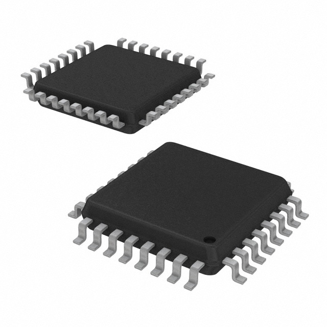
- Part No.:
- TW9960-TA1-GR
- Manufacturer:
- Renesas
- Category:
- Encoders, Decoders, Converters
- Package:
- 32-TQFP
- Datasheet:
-
 TW9960-TA1-GR.pdf
- Description:
- IC VIDEO DECODER 32TQFP
- Quantity:
- Payment:

- Shipping:

Inventory:2,033
Please send an inquiry. Send us your inquiry, and we will respond immediately.
Product details
Overview
TW9960-TA1-GR from Intersil is a low-power analog video decoder IC supporting NTSC/PAL with automatic format detection, 960H resolution output, ITU-R BT.656 YCbCr (4:2:2) digital video interface, and integrated 10-bit ADCs with 4-H adaptive comb filter. It operates from 1.8V/3.3V supplies, uses a single 36MHz crystal, and targets CCTV DVR front-end systems requiring high-fidelity composite video digitization.
For engineers reviewing the TW9960-TA1-GR datasheet, TW9960-TA1-GR pinout, TW9960-TA1-GR application, or TW9960-TA1-GR equivalent, key selection considerations include analog input flexibility (2× CVBS or 1× Y/C), programmable gain/white peak control, PAL delay line correction, sub-carrier PLL accuracy, and power-down mode support for embedded surveillance platforms.
Technical Context
The TW9960-TA1-GR integrates dual 10-bit ADCs with analog clamping and software-selectable input muxing, enabling simultaneous or independent processing of two CVBS or one Y/C signal. Its digital horizontal PLL ensures precise pixel sampling timing, while the digital sub-carrier PLL delivers stable color decoding across NTSC-M, NTSC-4.43, and multiple PAL variants (B/D/G/H/I/M/N/N-combination).
Advanced sync processing handles non-standard and weak analog signals without external circuitry. The 4-H adaptive comb filter separates luma/chroma with reduced cross-color artifacts, and the PAL delay line corrects color phase errors inherent in PAL-B/G/H broadcast signals.
Key Specifications
| Parameter | Value and Actual Design Meaning |
|---|---|
| Video Standards | NTSC-M, NTSC-4.43, PAL-B/D/G/H/I/M/N/N-combination with auto-detection |
| Analog Inputs | Software-selectable: 2× CVBS or 1× Y/C (S-Video) |
| ADC Resolution | Dual 10-bit ADCs with built-in analog anti-alias filtering |
| Output Format | ITU-R BT.656 compliant YCbCr (4:2:2), 8-bit parallel VD[7:0] |
| Power Supply | 1.8V core / 3.3V I/O; 3.3V-tolerant digital interface pins |
| Clock Source | Single 36MHz crystal supports all video standards without switching |
| Power Modes | Active, power-save, and full power-down modes with configurable entry/exit |
Pinout & Package
Package: 32-pin TQFP (7mm × 7mm, 0.8mm pitch), RoHS-compliant, lead-free.
| Pin/Terminal | Circuit Role | Design Meaning |
|---|---|---|
| VDD18 | Core power supply | 1.8V supply for internal logic and ADC core |
| VDD33 | I/O power supply | 3.3V supply for digital interface and I/O buffers |
| CIN0 | Analog video input | Primary composite video input (CVBS) or Y channel in Y/C mode |
| CIN1 | Analog video input | Secondary CVBS input or C channel in Y/C mode |
| VD[7:0] | Digital video output bus | 8-bit parallel YCbCr (4:2:2) data aligned to HSYNC/VSYNC |
| HSYNC | Horizontal sync output | Active-high sync pulse per line; used for timing video capture |
| VSYNC | Vertical sync output | Active-high field/frame sync; indicates start of new frame |
| SCLK/SDAT | 2-wire serial interface | I²C-compatible control interface (up to 400kHz) for register configuration |
| PDN | Power-down control | Active-low input to enter low-power state; retains register settings |
| RSTB | Hardware reset | Active-low asynchronous reset; initializes internal state machines |
Key Features
| Feature | Design Value |
|---|---|
| 4-H adaptive comb filter | Reduces cross-luminance and cross-color artifacts in composite video without external components |
| PAL delay line correction | Compensates for PAL-specific color phase shift, ensuring accurate hue reproduction across PAL-B/G/H |
| Programmable white peak control | Prevents overdriven luma clipping during high-contrast scenes in CCTV applications |
| Digital sub-carrier PLL | Maintains ±0.01% sub-carrier frequency stability for consistent color fidelity across temperature and voltage |
| Advanced sync processor | Locks to unstable or noisy analog signals (e.g., long coaxial cable runs) without frame drop or sync loss |
Applications
| High-Resolution CCTV DVR | Multi-Channel Video Encoder |
|---|---|
Use Scenario: Digitizing analog camera feeds in 960H resolution for storage and remote viewing. IC Role / Device Role / Timing Role: Primary video digitizer and format converter; provides synchronized YCbCr(4:2:2) output to SoC or FPGA. Use Value: Enables 960H analog-to-digital conversion with minimal external components and no external clock switching. | Use Scenario: Simultaneous encoding of up to 4 analog camera inputs in compact DVR hardware. IC Role / Device Role / Timing Role: Dual-input mux + dual ADC enables time-multiplexed or parallel analog video acquisition. Use Value: Reduces BOM count by integrating two 10-bit ADCs, clamping, AGC, and comb filtering in one 32-pin TQFP. |
| Embedded Vehicle DVR | Legacy Analog Monitor Interface |
Use Scenario: Recording analog dashcam feeds under wide temperature and vibration conditions. IC Role / Device Role / Timing Role: Low-power video front-end with power-down mode activated during vehicle ignition-off. Use Value: Draws <150mW in active mode and <10µA in power-down, extending battery-backed operation. | Use Scenario: Converting legacy NTSC/PAL outputs to digital for HDMI or LVDS display controllers. IC Role / Device Role / Timing Role: Standard-conforming ITU-R BT.656 bridge between analog video sources and digital display pipelines. Use Value: Eliminates need for external FIFO or timing controller due to embedded line-lock clock generator. |
Equivalent & Alternatives
The following parts are listed as comparable options for similar analog video decoder applications.
| Alternative Part | Technical Difference | Application Difference | Selection Advice |
|---|---|---|---|
| ADV7180BCPZ | Single 10-bit ADC; no dual-input mux; requires external crystal oscillator for PAL/NTSC switching | Limited to single CVBS input; lacks 960H support and PAL delay line correction | Preferred when system uses only one analog source and cost-per-channel is critical |
| TVP5150AM1IPBT | 10-bit ADC with SDRAM interface; no integrated 4-H comb filter; supports only NTSC/PAL-B/D/G | Requires external memory for line buffering; no white peak control or advanced sync handling | Chosen where external line memory is already present and PAL-H/I/N support is not required |
Compared with ADV7180BCPZ and TVP5150AM1IPBT, the TW9960-TA1-GR uniquely integrates dual analog inputs, 960H capability, PAL delay line, and single-crystal multi-standard operation-reducing layout complexity and improving robustness in multi-standard CCTV systems.
Availability
TW9960-TA1-GR is available at Aetrix Electronics and suitable for high-resolution CCTV DVRs, multi-channel video encoders, and embedded vehicle DVRs requiring stable component supply and long-term industrial availability.
Supply support for TW9960-TA1-GR includes scheduled delivery planning, volume procurement assistance, BOM continuity management, traceable sourcing, and lifecycle availability coordination for OEM customers, industrial embedded developers, connected-device designers, and electronics production programs.
Manufacturer
Intersil Corporation, now part of Renesas Electronics, designs precision analog and power management ICs with focus on reliability, thermal performance, and industrial-grade qualification.
The TW9960-TA1-GR belongs to Intersil's analog video interface product line, engineered specifically for cost-sensitive, space-constrained CCTV and security video systems needing high-fidelity composite video digitization.
FAQ
What video standards does the TW9960-TA1-GR support?
The TW9960-TA1-GR supports NTSC-M, NTSC-4.43, and PAL-B/D/G/H/I/M/N/N-combination with automatic format detection. It does not support SECAM or PAL-60. All standards operate from a single 36MHz crystal, eliminating the need for crystal switching or external PLL reconfiguration. The TW9960-TA1-GR's digital sub-carrier PLL maintains stable color decoding across all supported formats without manual intervention.
Does the TW9960-TA1-GR support 960H resolution output?
Yes, the TW9960-TA1-GR is explicitly designed for 960H analog video digitization, delivering 960×480 (PAL) or 960×488 (NTSC) effective resolution via its ITU-R BT.656 YCbCr (4:2:2) output. This exceeds standard D1 resolution and is optimized for high-density CCTV sensor outputs. The TW9960-TA1-GR achieves this using its dual 10-bit ADCs, adaptive comb filter, and line-lock clock generator-no external interpolation or scaling is required.
Can the TW9960-TA1-GR accept both CVBS and Y/C inputs simultaneously?
No-the TW9960-TA1-GR supports either two CVBS inputs or one Y/C (S-Video) pair, selected via software configuration of its internal analog mux. It cannot process CVBS and Y/C concurrently. Input selection is controlled through I²C register writes to the MUX0/MUX1 bits. The TW9960-TA1-GR's dual ADC architecture allows time-multiplexed or parallel acquisition depending on the chosen mode, but only one signal path is active per frame.
What power supply voltages does the TW9960-TA1-GR require?
The TW9960-TA1-GR requires two independent supplies: 1.8V for the core logic and ADC analog section (VDD18), and 3.3V for I/O and digital interface (VDD33). Its I/O pins are 3.3V-tolerant, allowing direct connection to 3.3V microcontrollers without level shifters. The TW9960-TA1-GR draws less than 150mW in active operation and enters sub-10µA power-down mode when PDN is asserted.
Is the TW9960-TA1-GR pin-compatible with other Intersil video decoders?
No, the TW9960-TA1-GR is not pin-compatible with earlier Intersil decoders such as the TW9910 or TW9920. Its 32-pin TQFP footprint, power pin allocation (separate VDD18/VDD33), and dedicated MPOUT/CLKX2 pins reflect a distinct layout optimized for 960H and dual-input operation. Board redesign is required when migrating to or from the TW9960-TA1-GR. The TW9960-TA1-GR datasheet must be consulted for exact routing and decoupling requirements.
TW9960-TA1-GR Specifications
- Product attributes
- Attribute value
- Manufacturer:
- Renesas
- Series:
- -
- Package/Case:
- 32-TQFP
- Packaging:
- Tray
- Product Status:
- Obsolete
- Type:
- Video Decoder
- Applications:
- -
- Voltage - Supply, Analog:
- 1.8V, 3.3V
- Voltage - Supply, Digital:
- 1.8V, 3.3V
- Grade:
- -
- Qualification:
- -
- Mounting Type:
- Surface Mount
- Supplier Device Package:
- 32-TQFP (5x5)
TW9960-TA1-GR FAQ
1.How can I place an order for TW9960-TA1-GR through Aetrix?
Please submit a Request for Quotation (RFQ) for TW9960-TA1-GR on Aetrix. Our sales agent will provide a competitive quotation and guide you through the order confirmation once you accept the terms.
2.Are the price and stock information for TW9960-TA1-GR reliable?
The price and inventory of TW9960-TA1-GR are updated periodically and may fluctuate due to market conditions. Stock and pricing data are typically refreshed every 24 hours. Quotation validity for TW9960-TA1-GR is usually 5 days.
3.What payment methods are accepted for TW9960-TA1-GR?
We accept Wire Transfer, PayPal, Credit Card, Western Union, MoneyGram, and Escrow for TW9960-TA1-GR transactions.
Note: Certain payment methods may incur a processing fee.
4.How is shipping managed for TW9960-TA1-GR?
TW9960-TA1-GR orders can be shipped via leading logistics carriers, including DHL, UPS, FedEx, TNT, or Registered Mail.
Once your TW9960-TA1-GR order is processed, you will receive an email with the shipment details and tracking number.
Note: Tracking information may take up to 24 hours to appear. Express delivery typically takes 3–5 business days.
5.How can I obtain technical support or documentation for TW9960-TA1-GR?
For technical support, including TW9960-TA1-GR datasheets, pinout diagrams, or application guidance, please contact our engineering support team. They can provide detailed documentation and assistance for your TW9960-TA1-GR requirements.
6.How does Aetrix verify that TW9960-TA1-GR is sourced from the original manufacturer or authorized distributors?
All TW9960-TA1-GR products on Aetrix are procured from qualified distributors and authorized channels. Our dedicated quality assurance team conducts strict verification, including traceability checks and, if necessary, third-party testing. This ensures that TW9960-TA1-GR meets industry standards.
7.What is the process for return or replacement of TW9960-TA1-GR?
All TW9960-TA1-GR units undergo pre-shipment inspection (PSI). If there is an issue with TW9960-TA1-GR, returns or replacements are accepted under the following conditions:
1.Quantity discrepancies, incorrect items, or visible external defects (such as breakage or corrosion), acknowledged by Aetrix.
2.The issue is reported within 90 days of delivery.
3.The TW9960-TA1-GR part is unused and in its original packaging.
Return procedure for TW9960-TA1-GR:
1.Submit a request within 90 days.
2.Obtain a Return Material Authorization (RMA) from Aetrix.
TW9960-TA1-GR Tags

-
MCP2120T-I/SL
Microchip Technology

-
LICAL-ENC-MS001
TE Connectivity Linx
-
TW9990AT-NA1-GR
Renesas
-
TVP5151IPBSR
Texas Instruments
-
TVP5150AM1IPBSR
Texas Instruments
-
LICAL-DEC-MS001-T
TE Connectivity Linx
-
ADV7391BCPZ
Analog Devices Inc.
-
ADV7393BCPZ-REEL
Analog Devices Inc.
-
ADV7393BCPZ
Analog Devices Inc.
-
ADV7391WBCPZ
Analog Devices Inc.
-
ADV7181DBCPZ
Analog Devices Inc.

-
ADV7181CBSTZ-REEL
Analog Devices Inc.
Tech Hub

TTL and CMOS logic families differ in thresholds, loading, output drive, power and timing. This engineering guide compares 74HC and 74HCT, calculates noise margins and checks 3.3 V/5 V compatibility.

A practical engineering guide to 3.3V and 5V logic compatibility, input thresholds, resistor dividers, translator ICs, MOSFET level shifting, I2C pull-ups, timing limits and power-sequencing risks.

The 74HC595 uses push-pull logic outputs, while the TPIC6B595 uses 50 V open-drain DMOS sinks for higher-power loads. This guide compares timing, current limits, 3.3 V interfacing, load wiring, thermal…

The 74HC595 converts serial data into eight stable parallel outputs. This guide covers pin functions, shift and storage timing, OE and MR behavior, drive-current limits, cascading, voltage compatibilit…

A technical comparison of level-sensitive latches and edge-triggered flip-flops, covering timing windows, setup and hold limits, master–slave operation, time borrowing, race-through, HDL inference and…

A D latch stores one bit while Enable controls when data can pass. This reference covers gate-level operation, truth tables, transparency, setup and hold timing, LE versus OE, common ICs and practical …

An SR latch stores one bit through cross-coupled feedback. This engineering reference covers NOR and NAND implementations, truth tables, forbidden-state recovery, gated operation, switch debouncing, fa…

Latch circuits retain one bit through feedback. This technical reference covers SR and D latches, truth tables, transparency, timing limits, latch-versus-flip-flop behavior, applications and common log…

An engineering guide to LED driver operation, constant-current and constant-voltage outputs, linear and switching topologies, dimming, IC selection, calculations, replacement compatibility, and fault c…

Operational amplifier guide covering op amp basics, feedback, ideal vs real op amps, common configurations, buffer circuits, offset, bias current, gain-bandwidth, slew rate, rail-to-rail limits and sel…


