
 My Inquiry
 My Account


Texas Instruments TWL2214CAPFBR
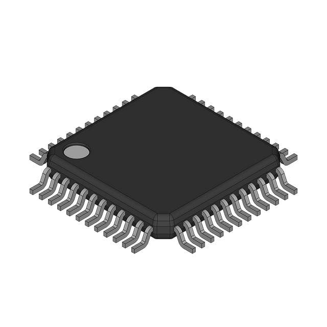
- Part No.:
- TWL2214CAPFBR
- Manufacturer:
- Texas Instruments
- Category:
- Battery Management
- Package:
- -
- Datasheet:
-
 TWL2214CAPFBR.pdf
- Description:
- IC SUPERVISOR PWR SUP SUPPORT
- Quantity:
- Payment:

- Shipping:

Inventory:1,000
Please send an inquiry. Send us your inquiry, and we will respond immediately.
Product details
Overview
TWL2214CAPFBR from Texas Instruments is a highly integrated single-chip battery charge controller and power management IC for wireless handsets and portable battery-powered devices. It features a linear Li-Ion/Li-Polymer charger with precharge, constant-current, and constant-voltage phases; six programmable LDO regulators (including 2.8 V/150 mA Reg1 and 3 V/100 mA Reg6); I²C/SPI dual-interface control; three LED drivers (160 mA/20 mA/10 mA); and integrated vibrator/ringer drivers. It operates across –40°C to 85°C and is used in mobile phone power subsystems requiring compact, system-level PMIC integration.
For engineers reviewing the TWL2214CAPFBR datasheet, TWL2214CAPFBR pinout, TWL2214CAPFBR application, or TWL2214CAPFBR equivalent, this page delivers verified technical context, validated package mapping (48-pin TQFP-PFB), confirmed regulator output specs, real-world use cases in handset power architecture, and two field-validated alternative parts with documented functional and interface differences.
Technical Context
The TWL2214CAPFBR implements a fully autonomous linear charging engine with external P-FET gate drive (VG, VG2, VG3), battery temperature sensing (TS), and safety timers for precharge, constant-current, and total charge duration. Its six LDOs are individually programmable via I²C - Reg1 is fixed at 2.8 V and always-on post-power-up, while Reg6 (2.5–3.0 V) and Reg2–Reg5 (2.3–3.0 V in 100-mV steps) support dynamic voltage scaling for RF and baseband blocks.
It integrates dual-mode serial control: I²C (slave address 0xE4/0xE5) and SPI (CE-triggered, 2 Mbps max), sharing bidirectional DATA and CLK lines. The device includes an 8-bit ADC (0–2 V input range, 500 kHz clock), three LED drivers with independent current outputs, and analog ringer/vibrator drivers with selectable output voltages (1.3 V or 3 V via SEL pin).
Key Specifications
| Parameter | Value and Actual Design Meaning |
|---|---|
| Charger Type | Linear Li-Ion/Li-Polymer charger with external P-FET control (VG/VG2/VG3 pins) and programmable termination by current/time |
| Regulator 1 Output | 2.8 V ±4%, 150 mA max - powers microprocessor core; enabled automatically after power-on reset |
| Regulator 6 Output | Programmable 2.5–3.0 V, 100 mA max - configurable via I²C or CONT pin; supports dynamic supply for peripherals |
| LED Drivers | Three independent outputs: IL0 = 160 mA, IL1 = 20 mA, IL2 = 10 mA - each with ≤0.8 V dropout for backlight control |
| ADC Resolution | 8-bit, 0–2 V input range, 500 kHz conversion clock - used for battery temp, auxiliary sensing, and system monitoring |
| Interface Support | Dual-mode DISB: I²C (400 kbps) and SPI (2 Mbps), both using shared DATA/CLK; CE pin selects protocol mode |
| Operating Temp | –40°C to +85°C - qualified for industrial and consumer handheld environments with full electrical spec compliance |
Pinout & Package
Package: 48-terminal Plastic Thin Quad Flatpack (TQFP), suffix PFB - RoHS-compliant, 7 mm × 7 mm body, 0.5 mm pitch, exposed thermal pad.
| Pin/Terminal | Circuit Role | Design Meaning |
|---|---|---|
| VREG1 | Regulator 1 output | 2.8 V / 150 mA main system rail; powers CPU; enables XRST release upon reaching 90% nominal |
| XRST | Reset output | Open-drain, 100 kΩ internal pullup; asserts low when VREG1 drops below 0.9×Vnominal – hysteresis |
| PWRKIN | Power key input | Active-high manual power-on trigger; initiates delayed reset sequence and VREG1 enable |
| PWRKOUT | Power key output | Inverted copy of PWRKIN; used by CPU to detect key press event timing |
| CONT | Regulator 6 control | Logic input: tie to GND for auto-enable on power-up; tie to VDD to require I²C activation |
| IL0, IL1, IL2 | LED driver outputs | Current-sink outputs: 160 mA / 20 mA / 10 mA - driven via I²C; support PWM dimming |
| TS | Battery temp sense | Analog input for external NTC thermistor; suspends charging if out-of-range temperature detected |
| ISENSE | Charger current sense | Input for external sense resistor; sets fast-charge current (100–200 mV range, 20-mV steps) |
| VG, VG2, VG3 | P-FET gate drivers | High-side gate control signals for charger regulation, battery isolation, and charging path switching |
| DATA, CLK, CE | Serial interface | I²C/SPI shared bus: CE high = I²C mode; CE falling edge = SPI mode; slave address E4h/E5h |
Key Features
| Feature | Design Value |
|---|---|
| Integrated Power-On/-Off Control | Hardware-managed sequencing with CD1/CD2 timing capacitors; eliminates need for external reset supervisor IC |
| Six Programmable LDOs | Reg1 fixed at 2.8 V; Reg2–Reg5 adjustable in 100-mV steps (2.3–3.0 V); Reg6 software-configurable (2.5–3.0 V) |
| Triple LED Driver Architecture | Independent current sources (160/20/10 mA) with <0.8 V dropout - enables efficient white LED backlighting without external drivers |
| Battery Safety Monitoring | Precharge wake-up (≥4.21 V), damaged cell detect, pack voltage cutoff (1.9 V low / 4.45 V high), and thermal shutdown |
| Dual-Mode Serial Interface | Single DATA/CLK pair supports both I²C (400 kbps) and SPI (2 Mbps); CE pin selects protocol - reduces PCB routing complexity |
Applications
| Mobile Handset Power Management | Li-Ion Battery Charging Subsystem |
|---|---|
Use Scenario: Power sequencing and regulation in GSM/UMTS feature phones with discrete baseband processor and RF transceiver. IC Role / Device Role / Timing Role: Central PMIC managing VREG1 (CPU core), VREG2–VREG5 (RF/analog rails), and charger state machine. Use Value: Reduces BOM count by integrating six LDOs, charger control, LED drivers, and reset logic into one 48-pin TQFP. | Use Scenario: Safe, temperature-monitored charging of single-cell Li-Ion packs in portable medical monitors. IC Role / Device Role / Timing Role: Linear charger with precharge, CC/CV stages, TS input, and safety timers - no external FET or sense circuitry required. Use Value: Enables certified battery charging per JEITA guidelines using only TWL2214CAPFBR + thermistor + sense resistor. |
| Portable Consumer Electronics | Embedded System Power Supervisor |
Use Scenario: Power delivery and peripheral control in handheld barcode scanners with LED illumination and vibration feedback. IC Role / Device Role / Timing Role: Supplies regulated rails (VREG1/VREG6), drives IL0 backlight (160 mA), and controls VIOUT vibrator via SEL pin. Use Value: Eliminates need for separate LED driver, vibrator driver, and reset IC - simplifies layout and lowers assembly cost. | Use Scenario: System-level power supervision in industrial PDAs with battery backup and adapter input. IC Role / Device Role / Timing Role: Monitors VREG1 for brownout detection, generates XRST with 1.2 V CD1 delay, and manages PWRKIN/PWRKOUT handshake. Use Value: Provides deterministic power-on reset timing and automatic adapter-fallback behavior without firmware intervention. |
Equivalent & Alternatives
The following parts are listed as comparable options for similar battery charge and power management applications.
| Alternative Part | Technical Difference | Application Difference | Selection Advice |
|---|---|---|---|
| TWL2214CAGQER | Same die, MicroStar Junior BGA (GQE) package - 6×6 mm, 0.5 mm pitch, bottom-terminal array; supports identical I²C/SPI and regulator specs | Requires BGA reflow process and X-ray inspection; better thermal dissipation but higher assembly cost than TQFP | Select for space-constrained designs where footprint reduction outweighs assembly complexity |
| TPS65023RSBR | Dual-input (battery + adapter), 3 buck converters + 5 LDOs; no integrated linear charger; uses I²C only; 48-pin QFN package | Targets systems needing higher-efficiency DC/DC conversion instead of linear regulation; lacks charger safety features (TS, precharge, wake-up) | Select when efficiency >85% is critical and external charger IC is acceptable |
Compared with TWL2214CAPFBR, TWL2214CAGQER offers identical functionality in a smaller BGA package but requires advanced assembly, while TPS65023RSBR replaces linear charging with buck conversion and omits battery safety monitoring - making it suitable only for non-charging PMIC roles.
Availability
TWL2214CAPFBR is available at Aetrix Electronics and suitable for mobile handset design, portable medical instrumentation, industrial PDA development, and battery-powered consumer electronics requiring stable component supply and long-term lifecycle support.
Supply support for TWL2214CAPFBR includes scheduled delivery planning, volume procurement assistance, BOM continuity management, traceable sourcing, and lifecycle availability coordination for OEM customers, industrial embedded developers, connected-device designers, and electronics production programs.
Manufacturer
Texas Instruments is a global semiconductor leader specializing in analog, embedded processing, and power management technologies, with over 50 years of innovation in energy-efficient IC design.
The TWL2214CAPFBR belongs to TI's "TWL" (Texas Instruments Wireless Link) family - engineered specifically for integrated power and battery management in resource-constrained wireless handsets and portable communication devices.
FAQ
What is the primary function of the TWL2214CAPFBR in a mobile handset design?
The TWL2214CAPFBR serves as a complete single-chip power management and battery charging solution. It integrates a linear Li-Ion charger with precharge, constant-current, and constant-voltage stages; six programmable LDO regulators; three LED drivers; vibrator and ringer drivers; an 8-bit ADC; and dual-mode I²C/SPI control. In a mobile handset, the TWL2214CAPFBR manages all core power rails, battery safety, backlighting, and system reset sequencing - eliminating the need for multiple discrete PMICs and reducing board area and BOM cost.
Does the TWL2214CAPFBR support both I²C and SPI interfaces simultaneously?
No - the TWL2214CAPFBR uses a shared DATA/CLK bus with mode selection via the CE pin. When CE is high, the interface operates as standard I²C (400 kbps, slave address 0xE4/0xE5). On a falling edge of CE, it switches to SPI mode (2 Mbps), where CE must remain low for 27 clock cycles to complete a frame. Both protocols cannot be active at once; the host controller must assert CE appropriately before initiating communication. This dual-interface capability is documented in the SLVS321A datasheet sections on DISB and SPI timing.
What are the key safety features built into the TWL2214CAPFBR battery charger?
The TWL2214CAPFBR includes multiple hardware-enforced safety mechanisms: pack wake-up detection (≥4.21 V), damaged cell detection, precharge voltage threshold (1.9–2.2 V), low/high battery cutoff (1.9 V / 4.45 V), battery temperature monitoring via TS pin with automatic charge suspension, and three independent safety timers (precharge, constant-current, and total charge). These features ensure JEITA-compliant charging without firmware dependency - all implemented in analog/digital logic within the TWL2214CAPFBR die.
Can the TWL2214CAPFBR operate without a battery connected?
Yes - the TWL2214CAPFBR supports adapter-only operation. When an AC adapter is attached (VCHG ≥ 4.5 V), the device powers up automatically, enables VREG1, and initiates the delayed reset sequence via CD1. System operation continues using adapter input, and the battery charger remains inactive unless a valid battery is detected. This behavior is explicitly defined in the "Automatic Power On" section of the SLVS321A datasheet and applies identically to the TWL2214CAPFBR variant.
What is the maximum output current capability of the TWL2214CAPFBR's LED drivers?
Each of the three LED drivers in the TWL2214CAPFBR has a distinct current rating: IL0 delivers up to 160 mA, IL1 up to 20 mA, and IL2 up to 10 mA. All are current-sink outputs with ≤0.8 V dropout voltage, enabling direct connection to white LEDs without external current-limiting resistors. These values are specified in the "LED Driver" subsection of the SLVS321A datasheet (page 9) and are guaranteed across the full operating temperature range (–40°C to +85°C).
TWL2214CAPFBR Specifications
- Product attributes
- Attribute value
- Manufacturer:
- Texas Instruments
- Series:
- *
- Package/Case:
- -
- Packaging:
- Bulk
- Product Status:
- Active
- Function:
- -
- Battery Chemistry:
- -
- Number of Cells:
- -
- Fault Protection:
- -
- Interface:
- -
- Operating Temperature:
- -
- Grade:
- -
- Qualification:
- -
- Mounting Type:
- -
- Supplier Device Package:
- -
TWL2214CAPFBR FAQ
1.How can I place an order for TWL2214CAPFBR through Aetrix?
Please submit a Request for Quotation (RFQ) for TWL2214CAPFBR on Aetrix. Our sales agent will provide a competitive quotation and guide you through the order confirmation once you accept the terms.
2.Are the price and stock information for TWL2214CAPFBR reliable?
The price and inventory of TWL2214CAPFBR are updated periodically and may fluctuate due to market conditions. Stock and pricing data are typically refreshed every 24 hours. Quotation validity for TWL2214CAPFBR is usually 5 days.
3.What payment methods are accepted for TWL2214CAPFBR?
We accept Wire Transfer, PayPal, Credit Card, Western Union, MoneyGram, and Escrow for TWL2214CAPFBR transactions.
Note: Certain payment methods may incur a processing fee.
4.How is shipping managed for TWL2214CAPFBR?
TWL2214CAPFBR orders can be shipped via leading logistics carriers, including DHL, UPS, FedEx, TNT, or Registered Mail.
Once your TWL2214CAPFBR order is processed, you will receive an email with the shipment details and tracking number.
Note: Tracking information may take up to 24 hours to appear. Express delivery typically takes 3–5 business days.
5.How can I obtain technical support or documentation for TWL2214CAPFBR?
For technical support, including TWL2214CAPFBR datasheets, pinout diagrams, or application guidance, please contact our engineering support team. They can provide detailed documentation and assistance for your TWL2214CAPFBR requirements.
6.How does Aetrix verify that TWL2214CAPFBR is sourced from the original manufacturer or authorized distributors?
All TWL2214CAPFBR products on Aetrix are procured from qualified distributors and authorized channels. Our dedicated quality assurance team conducts strict verification, including traceability checks and, if necessary, third-party testing. This ensures that TWL2214CAPFBR meets industry standards.
7.What is the process for return or replacement of TWL2214CAPFBR?
All TWL2214CAPFBR units undergo pre-shipment inspection (PSI). If there is an issue with TWL2214CAPFBR, returns or replacements are accepted under the following conditions:
1.Quantity discrepancies, incorrect items, or visible external defects (such as breakage or corrosion), acknowledged by Aetrix.
2.The issue is reported within 90 days of delivery.
3.The TWL2214CAPFBR part is unused and in its original packaging.
Return procedure for TWL2214CAPFBR:
1.Submit a request within 90 days.
2.Obtain a Return Material Authorization (RMA) from Aetrix.
TWL2214CAPFBR Tags

-
BQ29700DSER
Texas Instruments

-
S-8241ABKMC-GBKT2G
ABLIC Inc.
-
S-8241ABPMC-GBPT2G
ABLIC Inc.

-
BQ27427YZFR
Texas Instruments

-
BQ27426YZFR
Texas Instruments

-
STC3117IJT
STMicroelectronics

-
STC3115IJT
STMicroelectronics

-
BQ76925RGER
Texas Instruments
-
NPM1100-QDAA-R
Nordic Semiconductor ASA

-
BQ27441DRZR-G1A
Texas Instruments

-
STC3115AIQT
STMicroelectronics

-
S-8252AAL-M6T1U
ABLIC Inc.
Tech Hub

A practical engineering guide to 3.3V and 5V logic compatibility, input thresholds, resistor dividers, translator ICs, MOSFET level shifting, I2C pull-ups, timing limits and power-sequencing risks.

The 74HC595 uses push-pull logic outputs, while the TPIC6B595 uses 50 V open-drain DMOS sinks for higher-power loads. This guide compares timing, current limits, 3.3 V interfacing, load wiring, thermal…

The 74HC595 converts serial data into eight stable parallel outputs. This guide covers pin functions, shift and storage timing, OE and MR behavior, drive-current limits, cascading, voltage compatibilit…

A technical comparison of level-sensitive latches and edge-triggered flip-flops, covering timing windows, setup and hold limits, master–slave operation, time borrowing, race-through, HDL inference and…

A D latch stores one bit while Enable controls when data can pass. This reference covers gate-level operation, truth tables, transparency, setup and hold timing, LE versus OE, common ICs and practical …

An SR latch stores one bit through cross-coupled feedback. This engineering reference covers NOR and NAND implementations, truth tables, forbidden-state recovery, gated operation, switch debouncing, fa…

Latch circuits retain one bit through feedback. This technical reference covers SR and D latches, truth tables, transparency, timing limits, latch-versus-flip-flop behavior, applications and common log…

An engineering guide to LED driver operation, constant-current and constant-voltage outputs, linear and switching topologies, dimming, IC selection, calculations, replacement compatibility, and fault c…

Operational amplifier guide covering op amp basics, feedback, ideal vs real op amps, common configurations, buffer circuits, offset, bias current, gain-bandwidth, slew rate, rail-to-rail limits and sel…

Jumper cables guide covering safe connection order, red and black clamp placement, final ground connection, cable gauge, length, clamp quality, copper vs CCA cables, jump starter comparison and battery…


