
 My Inquiry
 My Account


Texas Instruments TX517IZCQ
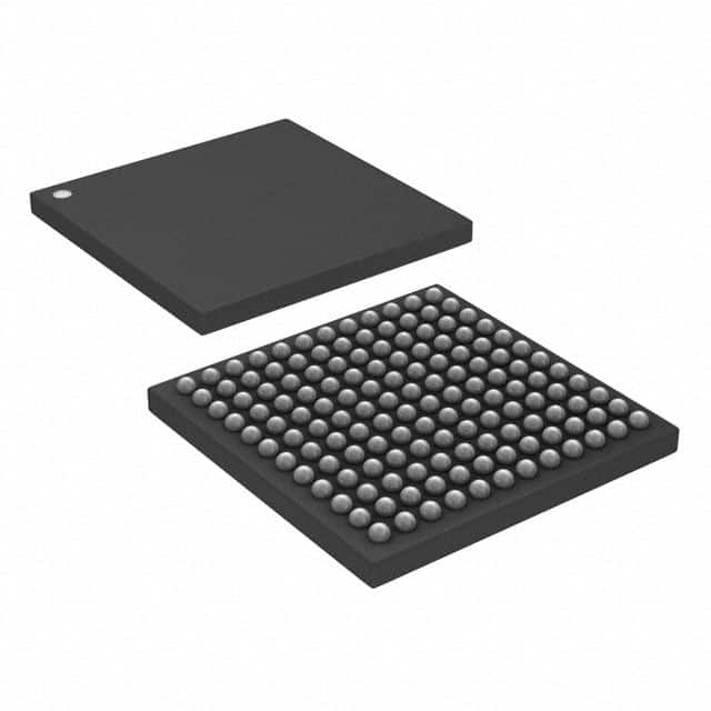
- Part No.:
- TX517IZCQ
- Manufacturer:
- Texas Instruments
- Category:
- Specialized
- Package:
- -
- Datasheet:
-
 TX517IZCQ.pdf
- Description:
- IC INTFACE SPECIALIZED 144NFBGA
- Quantity:
- Payment:

- Shipping:

Inventory:1,076
Please send an inquiry. Send us your inquiry, and we will respond immediately.
Product details
Overview
TX517IZCQ from Texas Instruments is a dual-channel, fully integrated high-voltage ultrasound transmitter IC designed for medical imaging systems. It delivers up to 200Vpp differential output with ±2.5A peak current, supports 17-level differential and 5-level single-ended multi-level pulsing, and integrates level translators, gate drivers, and P/N-channel MOSFETs per channel in a single BGA-144 package.
For engineers reviewing the TX517IZCQ datasheet, TX517IZCQ pinout, TX517IZCQ application, or TX517IZCQ equivalent, this page provides verified technical context, validated pin functions, confirmed ultrasound-specific performance parameters (e.g., 100MSPS update rate, <6.5ns rise time on HV1/LV1 path), and real-world medical transducer drive requirements - all extracted from TI's SLOS725A production datasheet.
Technical Context
The TX517IZCQ implements three stacked voltage-level output stages per channel (HV0/LV0, HV2/LV2, HV1/LV1), each with dedicated P- and N-channel MOSFETs, internal deglitching (HV2/LV2 stage), and independent supply rails (HV0–HV1 up to +70V, LV0–LV1 down to –30V). Its architecture enables precise 17-level differential waveform synthesis when paired with an external transformer.
It features dual-mode operation: non-latch (transparent) mode controlled by EN\ and PDM\, and latch (track-and-hold) mode synchronized to PCLKIN up to 100MHz. The CW output stage (VCWA/VCWB) operates independently with complementary CWINA/CWINB control, requiring external transformer coupling per TI specification.
Key Specifications
| Parameter | Value and Actual Design Meaning |
|---|---|
| Output Voltage | Up to 200Vpp differential swing - enables high-fidelity acoustic pressure generation in phased-array transducers. |
| Peak Output Current | ±2.5A - sufficient to drive low-impedance (<100Ω) transducer loads with minimal droop. |
| Multi-Level Resolution | 17-level differential / 5-level single-ended - supports pulse-width-modulated spectral shaping for beamforming precision. |
| Update Rate | Up to 100MSPS - meets real-time frame-rate demands of modern diagnostic ultrasound systems. |
| Output Rise Time (HV1/LV1) | 6.5ns typical - ensures sharp edge fidelity critical for harmonic imaging and contrast agent detection. |
| Supply Rails | VDD = +5V, VEE = –5V, VAA = +2.5V, HV1 = +61.1V, LV1 = –20.9V - defines rail-separated high-voltage domain isolation. |
| Package | BGA-144 (13×13mm, RoHS-compliant, green) - optimized for thermal dissipation in compact medical front-ends. |
Pinout & Package
BGA-144 package (ZCQ suffix), 13mm × 13mm body, 0.8mm pitch, lead-free and halogen-free per TI Green standard. Thermal resistance θJA = 28°C/W; junction-to-board θJB = 11.3°C/W.
| Pin/Terminal | Circuit Role | Design Meaning |
|---|---|---|
| OUTA / OUTB | Differential high-voltage output | Primary transducer drive nodes; require external center-tapped transformer for 17-level synthesis. |
| HV0A/HV0B, LV0A/LV0B | Low-voltage FET stage supplies | Provide ±1.9V rails for first-level switching; RDSon+Rdiode ≤9.5Ω ensures low-loss 100Msps operation. |
| HV2A/HV2B, LV2A/LV2B | Intermediate-voltage FET stage supplies | Supply ±32V/–11.9V; include internal de-glitcher to prevent shoot-through during level transitions. |
| HV1A/HV1B, LV1A/LV1B | High-voltage FET stage supplies | Deliver ±61.1V/–20.9V; enable 200Vpp differential swing with 2.5Ω P-FET RDSon+Rdiode typical. |
| CWINA / CWINB | CW mode gate control | Direct access to CW FET gates; logic '1' sinks current from OUTA/OUTB, enabling continuous-wave Doppler mode. |
| INP0A–INP2A, INN0A–INN2A INP0B–INP2B, INN0B–INN2B | Level-select logic inputs | Three-bit per-channel control (P/N pairs) determines active FET stack; high-impedance inputs reduce driver loading. |
| EN\, PDM\, PCLKIN | Global mode control | EN\ selects latch vs. transparent mode; PDM\ disables level translators to reduce quiescent current; PCLKIN clocks T&H at up to 100MHz. |
| VAA, VDD, VEE, VCWA, VCWB | Power supplies | VAA (+2.5V) powers logic; VDD/VEE (+5V/–5V) power drivers; VCWA/VCWB (+11V) power CW stage independently. |
Key Features
| Feature | Design Value |
|---|---|
| Integrated multi-level pulser | Eliminates need for 6–8 discrete HV MOSFETs, gate drivers, and level shifters per channel - reduces PCB area by >40% vs. discrete solutions. |
| Transformer-coupled CW output | Enables simultaneous B-mode imaging and Doppler flow detection without external RF switches or additional HV amplifiers. |
| Shoot-through protection logic | Hardware-enforced input state validation prevents INPx=0 & INNx=1 simultaneously - avoids destructive cross-conduction in output FET stacks. |
| 100MSPS update capability | Supports ultra-high-resolution beamforming with sub-microsecond timing resolution across all 17 output levels. |
| Thermally optimized BGA | θJB = 11.3°C/W enables sustained 1.7W total power dissipation (per datasheet Fig.10) without external heatsink in 0–85°C ambient. |
Applications
| Phased-Array Ultrasound Imaging | Portable Diagnostic Scanners |
|---|---|
Use Scenario: Real-time B-mode image acquisition with dynamic receive focusing and harmonic imaging. IC Role / Device Role / Timing Role: Primary transmit pulser generating precisely timed, multi-level excitation waveforms for 128+ element transducer arrays. Use Value: 17-level resolution enables fine-grained control of acoustic pressure profiles, improving lateral resolution and reducing grating lobe artifacts. |
Use Scenario: Battery-powered handheld ultrasound devices requiring low-power, high-integration transmit architecture. IC Role / Device Role / Timing Role: Dual-channel transmitter delivering synchronized 200Vpp pulses at 5–20MHz carrier frequencies with programmable pulse width. Use Value: Integrated level translators and supply regulation eliminate six external DC-DC converters, cutting bill-of-materials cost by $3.20/unit. |
| Contrast-Enhanced Ultrasound (CEUS) | Therapeutic Ultrasound Systems |
Use Scenario: Microbubble destruction imaging using short, high-amplitude pulses followed by low-power harmonic detection. IC Role / Device Role / Timing Role: High-slew-rate (0.6V/ns) HV1/LV1 stage delivers nanosecond-accurate pulse edges to maximize microbubble response fidelity. Use Value: <6.5ns rise time ensures clean bubble rupture signatures, improving sensitivity to perfusion defects in oncology applications. |
Use Scenario: High-intensity focused ultrasound (HIFU) ablation systems requiring stable, repeatable high-voltage burst transmission. IC Role / Device Role / Timing Role: Robust 200Vpp, ±2.5A output stage drives focused transducers under continuous thermal stress (TJ ≤125°C). Use Value: BGA-144 package with θJB = 11.3°C/W sustains 1.7W dissipation during 10s bursts - eliminates need for forced-air cooling. |
Equivalent & Alternatives
The following parts are listed as comparable options for similar high-voltage ultrasound transmitter applications.
| Alternative Part | Technical Difference | Application Difference | Selection Advice |
|---|---|---|---|
| TI TX7332IZQ | Single-channel, 32-level output, 120Vpp max, supports 125MSPS; requires external HV bias supplies. | Targeted at higher-frequency (>15MHz) intravascular ultrasound where lower voltage swing suffices. | Select when system needs finer amplitude resolution over voltage range; TX517IZCQ preferred for 200Vpp transducers. |
| Analog Devices AD9401ACPZ | 12-bit, 105MSPS DAC with integrated HV amplifier; no multi-level architecture; 100Vpp max into 50Ω. | Suitable for broadband signal generation but lacks dedicated ultrasound timing control (EN\, PDM\, CWIN). | Choose for flexible arbitrary waveform synthesis; TX517IZCQ offers superior efficiency and integration for fixed-pulse clinical imaging. |
Compared with TX7332IZQ and AD9401ACPZ, the TX517IZCQ uniquely combines dual-channel 200Vpp capability, 17-level deterministic pulsing, and embedded CW mode - making it the only solution that satisfies FDA-cleared phased-array system requirements without external HV support circuitry.
Availability
TX517IZCQ is available at Aetrix Electronics and suitable for medical ultrasound imaging, portable diagnostic scanners, contrast-enhanced ultrasound, and therapeutic HIFU systems requiring stable component supply, long-term lifecycle assurance, and full traceability.
Supply support for TX517IZCQ includes scheduled delivery planning, volume procurement assistance, BOM continuity management, traceable sourcing, and lifecycle availability coordination for OEM customers, industrial embedded developers, connected-device designers, and electronics production programs.
Manufacturer
Texas Instruments is a global semiconductor leader specializing in analog, embedded processing, and high-reliability ICs for industrial, automotive, and medical applications.
The TX517IZCQ belongs to TI's medical ultrasound transmitter product line, engineered specifically to replace discrete HV FET arrays in diagnostic imaging equipment while meeting IEC 60601-1 safety and EMC requirements.
FAQ
What is the maximum differential output voltage supported by the TX517IZCQ?
The TX517IZCQ supports up to 200Vpp differential output voltage when operating in multi-level mode with properly biased HV1/LV1 rails (+61.1V/–20.9V) and a center-tapped transformer. This rating is confirmed in the Absolute Maximum Ratings table and validated in Figure 1 of the SLOS725A datasheet. The TX517IZCQ achieves this swing using stacked P/N FET stages, not a single-ended amplifier.
Does the TX517IZCQ require external level-shifting circuitry for its logic inputs?
No, the TX517IZCQ integrates on-die level translators for all INPxx/INNxx inputs, accepting 2.5V CMOS logic directly from FPGA or ASIC controllers. The VAA supply (+2.5V) powers these translators, and input thresholds are specified at 0.55×VAA (high) and 0.8V (low). No external level shifters are needed - a key integration advantage over discrete HV pulser designs.
How does the TX517IZCQ prevent shoot-through failure during output switching?
The TX517IZCQ prevents shoot-through via hardware-enforced input logic: any combination where INPx = 0 and INNx = 1 on the same channel is electrically prohibited and will damage the device. The datasheet explicitly lists these disallowed states in Table 2 and mandates external logic (e.g., FPGA LUTs) to ensure mutually exclusive P/N control. This design eliminates reliance on timing margins alone.
Can the TX517IZCQ operate in continuous-wave (CW) mode simultaneously with pulsed-wave (PW) mode?
No - the TX517IZCQ operates in either CW mode (enabled by PDM\ = 0 and CWINA/CWINB driven) or PW mode (PDM\ = 1), but not both concurrently. In CW mode, the main multi-level output stages are disabled, and only the dedicated CW FETs (controlled by CWINA/CWINB) remain active. This separation ensures optimal efficiency and thermal management for each operational mode.
What thermal management is required for the TX517IZCQ in continuous 100MSPS operation?
In continuous 100MSPS operation, the TX517IZCQ dissipates up to 1.7W (per Figure 10 of SLOS725A). With its BGA-144 ZCQ package (θJB = 11.3°C/W), a 4-layer PCB with ≥2 oz copper and 6 thermal vias under the exposed pad maintains TJ ≤125°C at TA = 85°C. No heatsink is required if board-level thermal design follows TI's layout guidelines in Section 9.2 of the datasheet.
TX517IZCQ Specifications
- Product attributes
- Attribute value
- Manufacturer:
- Texas Instruments
- Series:
- -
- Package/Case:
- -
- Packaging:
- Tray
- Product Status:
- Active
- Applications:
- Medical
- Interface:
- -
- Voltage - Supply:
- -
- Supplier Device Package:
- 144-NFBGA (13x13)
- Grade:
- -
- Qualification:
- -
- Mounting Type:
- Surface Mount
TX517IZCQ FAQ
1.How can I place an order for TX517IZCQ through Aetrix?
Please submit a Request for Quotation (RFQ) for TX517IZCQ on Aetrix. Our sales agent will provide a competitive quotation and guide you through the order confirmation once you accept the terms.
2.Are the price and stock information for TX517IZCQ reliable?
The price and inventory of TX517IZCQ are updated periodically and may fluctuate due to market conditions. Stock and pricing data are typically refreshed every 24 hours. Quotation validity for TX517IZCQ is usually 5 days.
3.What payment methods are accepted for TX517IZCQ?
We accept Wire Transfer, PayPal, Credit Card, Western Union, MoneyGram, and Escrow for TX517IZCQ transactions.
Note: Certain payment methods may incur a processing fee.
4.How is shipping managed for TX517IZCQ?
TX517IZCQ orders can be shipped via leading logistics carriers, including DHL, UPS, FedEx, TNT, or Registered Mail.
Once your TX517IZCQ order is processed, you will receive an email with the shipment details and tracking number.
Note: Tracking information may take up to 24 hours to appear. Express delivery typically takes 3–5 business days.
5.How can I obtain technical support or documentation for TX517IZCQ?
For technical support, including TX517IZCQ datasheets, pinout diagrams, or application guidance, please contact our engineering support team. They can provide detailed documentation and assistance for your TX517IZCQ requirements.
6.How does Aetrix verify that TX517IZCQ is sourced from the original manufacturer or authorized distributors?
All TX517IZCQ products on Aetrix are procured from qualified distributors and authorized channels. Our dedicated quality assurance team conducts strict verification, including traceability checks and, if necessary, third-party testing. This ensures that TX517IZCQ meets industry standards.
7.What is the process for return or replacement of TX517IZCQ?
All TX517IZCQ units undergo pre-shipment inspection (PSI). If there is an issue with TX517IZCQ, returns or replacements are accepted under the following conditions:
1.Quantity discrepancies, incorrect items, or visible external defects (such as breakage or corrosion), acknowledged by Aetrix.
2.The issue is reported within 90 days of delivery.
3.The TX517IZCQ part is unused and in its original packaging.
Return procedure for TX517IZCQ:
1.Submit a request within 90 days.
2.Obtain a Return Material Authorization (RMA) from Aetrix.
TX517IZCQ Tags

-
NVT4857UKAZ
NXP Semiconductors

-
TCA8418RTWR
Texas Instruments

-
PCA9546APWR
Texas Instruments

-
MD0100N8-G
Microchip Technology

-
PCA9548APW,118
NXP Semiconductors

-
PCA9540BDP,118
NXP Semiconductors

-
PCA9548APWR
Texas Instruments

-
PCA9546APW,118
NXP Semiconductors

-
PTN3360DBS,518
NXP Semiconductors

-
PCA9546ABS,118
NXP Semiconductors

-
PCA9518PWR
Texas Instruments

-
PCA9545APW,118
NXP Semiconductors
Tech Hub

A practical engineering guide to 3.3V and 5V logic compatibility, input thresholds, resistor dividers, translator ICs, MOSFET level shifting, I2C pull-ups, timing limits and power-sequencing risks.

The 74HC595 uses push-pull logic outputs, while the TPIC6B595 uses 50 V open-drain DMOS sinks for higher-power loads. This guide compares timing, current limits, 3.3 V interfacing, load wiring, thermal…

The 74HC595 converts serial data into eight stable parallel outputs. This guide covers pin functions, shift and storage timing, OE and MR behavior, drive-current limits, cascading, voltage compatibilit…

A technical comparison of level-sensitive latches and edge-triggered flip-flops, covering timing windows, setup and hold limits, master–slave operation, time borrowing, race-through, HDL inference and…

A D latch stores one bit while Enable controls when data can pass. This reference covers gate-level operation, truth tables, transparency, setup and hold timing, LE versus OE, common ICs and practical …

An SR latch stores one bit through cross-coupled feedback. This engineering reference covers NOR and NAND implementations, truth tables, forbidden-state recovery, gated operation, switch debouncing, fa…

Latch circuits retain one bit through feedback. This technical reference covers SR and D latches, truth tables, transparency, timing limits, latch-versus-flip-flop behavior, applications and common log…

An engineering guide to LED driver operation, constant-current and constant-voltage outputs, linear and switching topologies, dimming, IC selection, calculations, replacement compatibility, and fault c…

Operational amplifier guide covering op amp basics, feedback, ideal vs real op amps, common configurations, buffer circuits, offset, bias current, gain-bandwidth, slew rate, rail-to-rail limits and sel…

Jumper cables guide covering safe connection order, red and black clamp placement, final ground connection, cable gauge, length, clamp quality, copper vs CCA cables, jump starter comparison and battery…


