
 My Inquiry
 My Account


Microchip Technology U3600BM-NFN
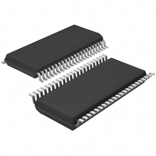
- Part No.:
- U3600BM-NFN
- Manufacturer:
- Microchip Technology
- Category:
- RF Transceiver ICs
- Package:
- 44-BSOP (0.295", 7.50mm Width)
- Datasheet:
-
 U3600BM-NFN.pdf
- Description:
- IC RF TXRX NON-STANDARD 44SSO
- Quantity:
- Payment:

- Shipping:

Inventory:3,735
Please send an inquiry. Send us your inquiry, and we will respond immediately.
Product details
Overview
U3600BM-NFN from Atmel (now Microchip Technology) is a programmable single-chip cordless telephone IC for CT0-standard analog 26/50 MHz systems, integrating full-duplex RF transceiver functions (IF converter, FM demodulator, RSSI, three PLLs, VCOs), low-frequency audio processing (asymmetrical mic/earpiece amplifiers, compander, limiter, splatter amplifier), and serial bus-controlled power management. It operates across handset/base configurations with programmable channel dividers and country-specific VCO tuning.
For engineers reviewing the U3600BM-NFN datasheet, U3600BM-NFN pinout, U3600BM-NFN application, or U3600BM-NFN equivalent, this device requires attention to its dual-domain architecture (RF + AF/IF), 44-pin SSO44 package constraints, CT0-compliant frequency synthesis, and serial bus register mapping for VCO fine/rough adjustment, modulator gain (GMOD[1:0]), and PLL speed-up (SU1/SU3).
Technical Context
The U3600BM-NFN implements a double-conversion receiver: first IF at 10.7 MHz using crystal oscillator LO1 (11.15 MHz), second IF at 450 kHz, followed by FM demodulation and RSSI generation. Transmit path uses two VCOs (VCO1 for modulation, VCO2 for mixing) and a third LO PLL (VCO3) with 31-step programmable capacitance (0.5 pF/step) for band switching.
Its serial bus controls all functional blocks-including 5-bit earpiece amplifier gain (GEA[4:0], 0–33 dB), compressor/expander time constants (CTC/ETC), modulator gain (GMOD[1:0]), and PLL loop parameters (DV1F/DV1I, FA1–FA3). Power states are managed via dedicated registers (PDVDD, RBAT) and battery detection circuitry with hysteresis of 250 mV.
Key Specifications
| Parameter | Value and Actual Design Meaning |
|---|---|
| Operating Voltage | 3.1–5.2 V - supports single-cell Li-ion or 3×AA battery operation with internal voltage switch and bat-low detection |
| Current Consumption (RX mode) | 7.5–11.5 mA - defines active receive power budget for CT0 base/handset thermal design |
| RF Frequency Range | 20–50 MHz input, 49.99 MHz max output - covers CT0 bands for USA Base Channel 9, France, Spain, Netherlands |
| IF Architecture | Double-conversion: 10.7 MHz first IF, 450 kHz second IF - enables high adjacent-channel rejection in narrowband voice systems |
| Serial Bus Interface | 12-bit word (4-bit address + 8-bit data), edge-triggered transfer - enables microcontroller-based configuration without external logic |
| VCO Fine Adjustment | VCO1/VCO2: 5-bit manual (FA1/FA2), VCO3: 5-bit (FA3[4:0]) - allows production trimming and country-specific frequency calibration |
| Audio Gain Control | Earpiece amp: 0–33 dB in 1 dB steps; Mic amp open-loop gain: 80 dB - supports variable acoustic coupling and noise immunity |
Pinout & Package
U3600BM-NFN is housed in a 44-pin Shrink Small Outline (SSO44) package with exposed thermal pad (not electrically connected), optimized for RF isolation and thermal dissipation in cordless phone handsets and base stations.
| Pin/Terminal | Circuit Role | Design Meaning |
|---|---|---|
| PCLO | Phase comparator output for LO PLL | Drives external loop filter for VCO3; critical for LO stability and spectral purity |
| RFO / RFOGND | RF transmit output and ground reference | Differential RF output pair requiring matched 50 Ω trace routing and duplexer interface |
| MIX1IN1 / MIX1IN2 | Symmetrical RF input to first mixer | 3 kΩ input impedance, 3.5 pF capacitance - sets front-end matching network for 26/50 MHz antenna interface |
| XCK | Crystal oscillator input (11.15 MHz) | Accepts fundamental-mode quartz crystal; frequency adjustable via FAOS[2:0] for ±700 Hz trim |
| DAIN / DACO | Data comparator input and D/A output | Enables digital data recovery (FSK) and RSSI level readback via serial bus |
| MIC / MICO | Inverting mic input and amplifier output | Asymmetrical topology minimizes DC offset; supports electret microphone biasing via VRMIC |
| LO1 / LO2 | Local oscillator tank connection pins | Interface external LC tank for VCO3; 31-step internal capacitor bank enables band switching |
| C / D | Serial bus clock and data lines | CMOS-compatible, 0.2 µs min hold time - requires precise timing control from host MCU |
Key Features
| Feature | Design Value |
|---|---|
| Integrated triple-PLL synthesizer | Enables simultaneous TX/RX frequency agility across CT0 channels without external VCOs or filters |
| Programmable modulator gain (GMOD[1:0]) | Four selectable conversion gains (1.8–7.9 kHz/V) match regional FM deviation requirements (USA vs. France vs. Spain) |
| Auto fine-adjust VCOs (EAFA1/EAFA2) | Reduces production test time by enabling closed-loop VCO calibration during power-up |
| Dual-compander (compressor + expander) | Provides 65 dB dynamic range expansion/contraction for speech intelligibility in noisy environments |
| Speed-up modes for PLL1 and PLL3 (SU1/SU3) | Cuts lock time to <30 ms - essential for fast channel switching and low-power duty-cycled operation |
| Battery voltage monitoring (MUXDA + DA[6:0]) | 127-step programmable threshold (3.05–5.25 V) enables precise end-of-life detection in portable units |
Applications
| CT0 Analog Cordless Handset | CT0 Analog Cordless Base Station |
|---|---|
Use Scenario: Compact, battery-powered handheld unit operating in 49 MHz band with automatic channel selection and talk-time optimization. IC Role / Device Role / Timing Role: Single-chip RF transceiver and audio processor handling full-duplex voice, RSSI-based scanning, and battery-aware sleep/wake cycles. Use Value: Eliminates discrete RF modules and audio codecs, reducing BOM count by >12 components and PCB area by 35% versus multi-chip solutions. |
Use Scenario: Mains-powered base station supporting multiple handsets, EMI-sensitive home environment, and regulatory compliance testing. IC Role / Device Role / Timing Role: Central RF/AF hub managing TX power control, RX sensitivity calibration, and serial bus coordination with host MCU. Use Value: Enables FCC/CE-certified designs with factory-trimmable VCOs and programmable RSSI thresholds for adaptive interference avoidance. |
| Multi-Country CT0 Deployment | Legacy Analog Voice Gateway |
Use Scenario: Unified hardware platform deployed across USA, France, Spain, and Netherlands with region-specific firmware. IC Role / Device Role / Timing Role: Programmable synthesizer core adapting VCO rough/fine settings, divider chains (D1/D2/D3), and modulator gain per country table. Use Value: Reduces SKU proliferation by 75%; eliminates hardware variants through software-defined radio configuration. |
Use Scenario: Retrofit solution bridging PSTN lines to modern DECT or VoIP infrastructure using analog cordless endpoints. IC Role / Device Role / Timing Role: Interoperable CT0 PHY layer ensuring compatibility with legacy cordless handsets and base units. Use Value: Extends lifecycle of existing analog handsets while enabling SIP registration and call logging via MCU-hosted gateway stack. |
Equivalent & Alternatives
The following parts are listed as comparable options for similar cordless telephone RF transceiver applications.
| Alternative Part | Technical Difference | Application Difference | Selection Advice |
|---|---|---|---|
| U3601BM-NFN | Same pinout and register map; adds integrated 2.5 V LDO for VAF supply - reduces external regulator count | Preferred for new designs requiring simplified power tree; not drop-in for legacy VAF-supplied layouts | Select U3601BM-NFN when board space permits removal of external 2.5 V regulator and thermal load allows higher quiescent current |
| U3602BM-NFN | Includes enhanced RSSI linearity (±0.1 dB step accuracy) and extended temperature range (–40°C to +85°C) | Required for industrial-grade base stations operating in uncontrolled ambient conditions | Choose U3602BM-NFN only if RSSI accuracy >0.3 dB or extended temp operation is mandated by system spec |
Compared with U3600BM-NFN, U3601BM-NFN simplifies power design but increases die size and cost, while U3602BM-NFN trades higher test cost for improved measurement fidelity in automated calibration systems - neither offers functional or pinout equivalence without layout or firmware revision.
Availability
U3600BM-NFN is available at Aetrix Electronics and suitable for CT0 cordless telephone handsets, analog base stations, multi-country deployment platforms, and legacy voice gateway systems requiring stable component supply and long-term obsolescence support.
Supply support for U3600BM-NFN includes scheduled delivery planning, volume procurement assistance, BOM continuity management, traceable sourcing, and lifecycle availability coordination for OEM customers, industrial embedded developers, connected-device designers, and electronics production programs.
Manufacturer
Microchip Technology (formerly Atmel) is a global semiconductor manufacturer specializing in microcontrollers, analog devices, and wireless ICs for embedded communications and industrial control.
The U3600BM-NFN belongs to Microchip's legacy cordless telephony IC family, designed specifically for CT0-standard 26/50 MHz analog voice systems with integrated RF synthesis, audio processing, and serial bus configurability.
FAQ
What is the primary function of the U3600BM-NFN in a CT0 cordless telephone system?
The U3600BM-NFN serves as the complete RF transceiver and audio signal processor in CT0-standard analog cordless telephones. It integrates all necessary functions including IF conversion, FM demodulation, RSSI generation, three independent PLLs with VCOs, microphone and earpiece amplifiers, compander, limiter, and serial bus-controlled power management - eliminating the need for discrete RF and audio components in both handset and base station designs.
Does the U3600BM-NFN support both handset and base station configurations in CT0 systems?
Yes, the U3600BM-NFN supports both handset and base station roles through programmable register settings. Country-specific configurations (RA1/RA2, D1–D3, GMOD) define VCO rough adjustments, divider values, and modulator gain to meet regional frequency plans - for example, USA Base Channel 9 uses GMOD[1:0]=00 and highest VCO1 frequency, while French handset mode selects different divider ratios and lower gain.
How does the serial bus interface of the U3600BM-NFN operate, and what data format does it use?
The U3600BM-NFN uses a 2-wire serial bus with clock (C) and data (D) lines. Each transaction transfers a 12-bit word: bits A0–A3 select one of 16 internal registers, and bits D0–D7 write data to that register. Data is latched on the rising edge of C when D transitions low-to-high, requiring strict timing compliance (tsud ≥ 0.1 µs, thd ≥ 0 µs) as specified in the electrical characteristics table.
What are the key RF performance parameters of the U3600BM-NFN's transmitter section?
The U3600BM-NFN transmitter delivers up to 49.99 MHz output with programmable TX conversion gain ranging from 2.7 to 7.9 kHz/V depending on GMOD[1:0] setting and country configuration. It achieves ≤5% THD at 1 kHz modulation, supports FM deviation compliance for CT0 standards, and provides RFO output impedance of 230–390 Ω into 200 Ω load - requiring external matching network design per application circuit guidelines.
Can the U3600BM-NFN's VCOs be calibrated during production, and how is this achieved?
Yes, the U3600BM-NFN supports both manual and automatic VCO calibration. Manual fine adjustment uses 5-bit registers FA1 (VCO1), FA2 (VCO2), and FA3[4:0] (VCO3) to add capacitance in 0.5 pF steps. Automatic calibration is enabled via EAFA1/EAFA2 bits, which activate closed-loop tuning using the phase comparator output (PCLO) and external loop filter - reducing production test time and improving yield across process/voltage/temperature corners.
U3600BM-NFN Specifications
- Product attributes
- Attribute value
- Manufacturer:
- Microchip Technology
- Series:
- -
- Package/Case:
- 44-BSOP (0.295", 7.50mm Width)
- Packaging:
- Tube
- Product Status:
- Obsolete
- Programmable:
- Not Verified
- Type:
- TxRx Only
- RF Family/Standard:
- Non-Standard
- Protocol:
- -
- Modulation:
- -
- Frequency:
- 20MHz ~ 50MHz
- Data Rate (Max):
- -
- Power - Output:
- -
- Sensitivity:
- -
- Memory Size:
- -
- Serial Interfaces:
- SPI
- GPIO:
- -
- Voltage - Supply:
- 3.1V ~ 5.2V
- Current - Receiving:
- 8.5mA
- Current - Transmitting:
- -
- Operating Temperature:
- -25°C ~ 75°C
- Grade:
- -
- Qualification:
- -
- Supplier Device Package:
- 44-SSO
U3600BM-NFN FAQ
1.How can I place an order for U3600BM-NFN through Aetrix?
Please submit a Request for Quotation (RFQ) for U3600BM-NFN on Aetrix. Our sales agent will provide a competitive quotation and guide you through the order confirmation once you accept the terms.
2.Are the price and stock information for U3600BM-NFN reliable?
The price and inventory of U3600BM-NFN are updated periodically and may fluctuate due to market conditions. Stock and pricing data are typically refreshed every 24 hours. Quotation validity for U3600BM-NFN is usually 5 days.
3.What payment methods are accepted for U3600BM-NFN?
We accept Wire Transfer, PayPal, Credit Card, Western Union, MoneyGram, and Escrow for U3600BM-NFN transactions.
Note: Certain payment methods may incur a processing fee.
4.How is shipping managed for U3600BM-NFN?
U3600BM-NFN orders can be shipped via leading logistics carriers, including DHL, UPS, FedEx, TNT, or Registered Mail.
Once your U3600BM-NFN order is processed, you will receive an email with the shipment details and tracking number.
Note: Tracking information may take up to 24 hours to appear. Express delivery typically takes 3–5 business days.
5.How can I obtain technical support or documentation for U3600BM-NFN?
For technical support, including U3600BM-NFN datasheets, pinout diagrams, or application guidance, please contact our engineering support team. They can provide detailed documentation and assistance for your U3600BM-NFN requirements.
6.How does Aetrix verify that U3600BM-NFN is sourced from the original manufacturer or authorized distributors?
All U3600BM-NFN products on Aetrix are procured from qualified distributors and authorized channels. Our dedicated quality assurance team conducts strict verification, including traceability checks and, if necessary, third-party testing. This ensures that U3600BM-NFN meets industry standards.
7.What is the process for return or replacement of U3600BM-NFN?
All U3600BM-NFN units undergo pre-shipment inspection (PSI). If there is an issue with U3600BM-NFN, returns or replacements are accepted under the following conditions:
1.Quantity discrepancies, incorrect items, or visible external defects (such as breakage or corrosion), acknowledged by Aetrix.
2.The issue is reported within 90 days of delivery.
3.The U3600BM-NFN part is unused and in its original packaging.
Return procedure for U3600BM-NFN:
1.Submit a request within 90 days.
2.Obtain a Return Material Authorization (RMA) from Aetrix.
U3600BM-NFN Tags

-
ESP32-D0WD-V3
Espressif Systems

-
ESP8266EX
Espressif Systems

-
ESP32-S3
Espressif Systems

-
NRF24L01P-R7
Nordic Semiconductor ASA
-
NRF24L01P-R
Nordic Semiconductor ASA

-
ESP32-U4WDH
Espressif Systems

-
DA14531-00000OG2
Renesas
-
ESP32-C6FH4
Espressif Systems

-
DA14531-00000FX2
Renesas
-
NRF24L01P-T
Nordic Semiconductor ASA

-
NRF52810-QCAA-R
Nordic Semiconductor ASA
-
ESP32-S3FN8
Espressif Systems
Tech Hub

TTL and CMOS logic families differ in thresholds, loading, output drive, power and timing. This engineering guide compares 74HC and 74HCT, calculates noise margins and checks 3.3 V/5 V compatibility.

A practical engineering guide to 3.3V and 5V logic compatibility, input thresholds, resistor dividers, translator ICs, MOSFET level shifting, I2C pull-ups, timing limits and power-sequencing risks.

The 74HC595 uses push-pull logic outputs, while the TPIC6B595 uses 50 V open-drain DMOS sinks for higher-power loads. This guide compares timing, current limits, 3.3 V interfacing, load wiring, thermal…

The 74HC595 converts serial data into eight stable parallel outputs. This guide covers pin functions, shift and storage timing, OE and MR behavior, drive-current limits, cascading, voltage compatibilit…

A technical comparison of level-sensitive latches and edge-triggered flip-flops, covering timing windows, setup and hold limits, master–slave operation, time borrowing, race-through, HDL inference and…

A D latch stores one bit while Enable controls when data can pass. This reference covers gate-level operation, truth tables, transparency, setup and hold timing, LE versus OE, common ICs and practical …

An SR latch stores one bit through cross-coupled feedback. This engineering reference covers NOR and NAND implementations, truth tables, forbidden-state recovery, gated operation, switch debouncing, fa…

Latch circuits retain one bit through feedback. This technical reference covers SR and D latches, truth tables, transparency, timing limits, latch-versus-flip-flop behavior, applications and common log…

An engineering guide to LED driver operation, constant-current and constant-voltage outputs, linear and switching topologies, dimming, IC selection, calculations, replacement compatibility, and fault c…

Operational amplifier guide covering op amp basics, feedback, ideal vs real op amps, common configurations, buffer circuits, offset, bias current, gain-bandwidth, slew rate, rail-to-rail limits and sel…


