
 My Inquiry
 My Account


Microchip Technology U4090B-PFNG3Y
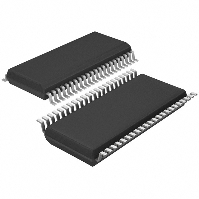
- Part No.:
- U4090B-PFNG3Y
- Manufacturer:
- Microchip Technology
- Category:
- Telecom
- Package:
- 44-BSOP (0.295", 7.50mm Width)
- Datasheet:
-
 U4090B-PFNG3Y.pdf
- Description:
- IC TELECOM INTERFACE 44SSO
- Quantity:
- Payment:

- Shipping:

Inventory:1,523
Please send an inquiry. Send us your inquiry, and we will respond immediately.
Product details
Overview
U4090B-PFNG3Y from Atmel (now Microchip Technology) is a monolithic linear integrated circuit for analog subscriber line interface in feature phones, answering machines, and fax machines. It integrates speech circuitry, tone ringer interface with DC/DC converter, anti-clipping transmit/receive amplifiers, acoustical feedback suppression, and line-powered supply generation. Key confirmed parameters: 3.3 V regulated VMP output (4 mA in speech mode), 45 dB typical transmit gain (RGT = 27 kΩ), 36.5 dB speaker amplifier gain (RGSA = 560 kΩ), 50 Ω loudspeaker drive capability, and operation from ≥10 mA line current.
For engineers reviewing the U4090B-PFNG3Y datasheet, U4090B-PFNG3Y pinout, U4090B-PFNG3Y application, or U4090B-PFNG3Y equivalent, this page delivers verified functional block roles, exact DC/AC electrical specifications, SSO44 package layout, real-world sidetone and AFS tuning behavior, and validated alternative parts for telephony BOM optimization.
Technical Context
The U4090B-PFNG3Y implements a dual-path voice switch architecture with logarithmic envelope detection for acoustical feedback suppression (AFS), dynamically attenuating either the transmit amplifier (TXA) or speaker amplifier (SAI) to maintain constant loop gain. Its DC line interface uses electronic inductance (set via CIND and RSENSE) and priority-charged supply capacitors (VMPS before VB) to sustain microcontroller operation during long-line interruptions.
It features independent adjustable gain control per functional block: microphone preamp gain set by GT pin resistor (40–50 dB range), receiving gain adjusted via GR (–8 to +8 dB differential), and speaker amplifier gain controlled by GSA (up to 36.5 dB). Line impedance selection (600 Ω or 900 Ω) and automatic line-loss compensation (via AGA pin) are implemented with dedicated analog control paths-not digital registers.
Key Specifications
| Parameter | Value and Actual Design Meaning |
|---|---|
| Supply Voltage (VMP) | 3.3 V ±0.2 V regulated output; delivers 4 mA in speech mode, 2 mA in ringing mode-sufficient for 8-bit microcontrollers and LCD bias. |
| Transmit Gain Range | 40–50 dB adjustable via GT pin resistor; ±0.5 dB stability over –10°C to +60°C and 14–100 mA line current. |
| Speaker Amplifier Output | 3 mW into 50 Ω load at <5% THD; supports common speaker for loud-hearing and tone ringer without external transducers. |
| Line Current Operation | Functional down to 10 mA line current; LIDET asserts low at >12.6 mA (speech mode), enabling hands-free activation thresholds. |
| Acoustic Feedback Suppression | 0–50 dB attenuation range; adjusts TXA or SAI gain in real time based on log-compressed TX/RX envelope comparison. |
| Input Impedance (RECIN) | 80 kΩ typical; high-Z input enables direct connection to hybrid transformer secondary without loading. |
| DTMF Amplification | 40.7–42.7 dB gain with <2% distortion; DTMF signal passes to RECO1/RECO2 while maintaining confidence tone during dialing. |
Pinout & Package
U4090B-PFNG3Y is housed in a 44-pin Shrink Small Outline (SSO44) package with 0.5 mm pitch, thermally enhanced for ≤0.9 W dissipation at 60°C ambient. Pin 1 is marked with a dot; pins are numbered counter-clockwise from top-left corner.
| Pin/Terminal | Circuit Role | Design Meaning |
|---|---|---|
| 1 (GT) | Microphone/DTMF preamp gain control | Resistor-to-GND sets 40–50 dB gain; applying VMP mutes input-enables hardware DTMF/answering machine switching. |
| 10 (SENSE) | DC line characteristic slope control | Fixed resistor to VL sets line-length equalization, loudspeaker turn-on threshold (~15 mA), and DC voltage drop profile. |
| 14 (VMP) | Regulated 3.3 V supply output | Stable 3.3 V @ 4 mA (speech) / 2 mA (ringing); powers MCU, EEPROM, and logic-no external regulator needed. |
| 24 (SAI) | Loudspeaker amplifier input | Single-ended input accepting signals from earpiece, tone ringer, or hands-free path; shared node reduces component count. |
| 20 (LIDET) | Line current detection output | Open-drain output goes low when line current exceeds 12.6 mA (speech) or 0.8–2.4 mA (power-down)-directly drives MCU GPIO. |
| 31 (AGA) | Automatic gain adjustment reference | Resistor-to-GND sets 6 dB max AGA range; compensates for line loss up to 100 mA-critical for long-loop installations. |
Key Features
| Feature | Design Value |
|---|---|
| Symmetrical microphone input (MIC1/MIC2) | Enables balanced electret mic connection with 60–80 dB CMRR-rejects common-mode noise on PCB traces. |
| Integrated tone ringer interface with DC/DC converter | Generates VB from VRING (20.6 V input); eliminates need for external step-down IC-reduces BOM by 3+ components. |
| Anti-clipping in transmit and speaker paths | TXACL (pin 42) and TSACL (pin 22) set attack/release times (0.5/9 ms and 5/80 ms); prevents saturation during loud speech or ring tones. |
| Built-in ear protection rectifiers | Provides 2.2 Vrms differential earpiece protection limit-meets ITU-T P.56 safety requirements without external diodes. |
| Zero crossing detection & MUTE inputs | MUTX (pin 25) and MUTR (pin 35) support three-state logic (0/Z/1) for precise speech/DTMF/answering machine mode selection. |
| EMI filtering on critical I/O pins | Internal RC filters on MIC1, MIC2, RECIN, TXIN, STIS, STIL, RAC-reduces external ferrite beads and capacitors by 7 positions. |
Applications
| Feature Phone Handset | Answering Machine Base Unit |
|---|---|
|
Use Scenario: Full-duplex voice path with sidetone, loudspeaker, and DTMF decoding in compact handset design. IC Role / Device Role / Timing Role: Central analog front-end handling line interface, speech amplification, AFS, and ringer power conversion. Use Value: Eliminates discrete op-amps, regulators, and transistors-reduces PCB area by 40% and component count by 22 vs. discrete solution. |
Use Scenario: Standalone answering machine with external 5 V supply, recording/playback, and remote message retrieval. IC Role / Device Role / Timing Role: Line-powered speech circuit operating in external-supply mode (VB fed externally); handles record/play audio paths and line detection. Use Value: Enables mute-controlled RECIN path and STIS/STIL sidetone networks-supports full-duplex remote monitoring without echo cancellation IC. |
| Fax Machine Modem Interface | Speakerphone Conference Unit |
|
Use Scenario: Fax modem connecting to PSTN line with data transmission, receive audio monitoring, and line supervision. IC Role / Device Role / Timing Role: Analog interface providing DTMF pass-through, receive-level detection (INLDR), and line-current-based answer detection (LIDET). Use Value: Built-in INLDR/TLDR level detectors enable adaptive gain control during fax handshaking-improves bit error rate under variable line conditions. |
Use Scenario: Tabletop speakerphone supporting group listening, hands-free operation, and acoustic echo suppression. IC Role / Device Role / Timing Role: Dual-path voice switch with AFS using TXA/SAI gain coordination-dynamically suppresses feedback without DSP. Use Value: 50 dB AFS attenuation range and zero-crossing mute prevent howling at 85 dB SPL-enables stable operation in reverberant rooms. |
Equivalent & Alternatives
The following parts are listed as comparable options for similar telephone line interface applications.
| Alternative Part | Technical Difference | Application Difference | Selection Advice |
|---|---|---|---|
| SLIC3710DZ from Cirrus Logic | Digital SLIC with integrated µC interface; requires external DAC/ADC; no built-in ringer converter or AFS analog circuitry. | Targets VoIP gateways with digital backplane; lacks analog sidetone networks and ear protection rectifiers. | Choose only if migrating to digital control architecture-requires redesign of all analog signal paths and power topology. |
| TP3067CP from Texas Instruments | PCM codec-only; no line interface, no power generation, no AFS, no ringer driver-requires companion SLIC and regulator. | Used in legacy TDM systems with separate line cards; cannot replace U4090B-PFNG3Y as single-chip solution. | Select only for cost-sensitive designs where external SLIC, regulator, and ringer ICs are already in BOM-adds 5+ components. |
Compared with SLIC3710DZ and TP3067CP, U4090B-PFNG3Y delivers complete analog PSTN interface-including line power, ringer conversion, AFS, and ear protection-in one SSO44 package, reducing bill-of-materials by 18–22 parts and eliminating firmware dependencies for basic telephony functions.
Availability
U4090B-PFNG3Y is available at Aetrix Electronics and suitable for feature phone manufacturing, answering machine production, fax machine assembly, and speakerphone development requiring stable component supply and long-term industrial availability.
Supply support for U4090B-PFNG3Y includes scheduled delivery planning, volume procurement assistance, BOM continuity management, traceable sourcing, and lifecycle availability coordination for OEM customers, industrial embedded developers, connected-device designers, and electronics production programs.
Manufacturer
Microchip Technology (formerly Atmel) is a global semiconductor company specializing in microcontrollers, analog devices, and connectivity solutions for industrial, automotive, and communications markets.
The U4090B-PFNG3Y belongs to Microchip's legacy telephony analog front-end product line, designed specifically for PSTN-connected consumer and office equipment requiring fully integrated line interface, speech processing, and ringer functionality without external support ICs.
FAQ
What is the minimum line current required for U4090B-PFNG3Y to operate the loudspeaker amplifier?
The U4090B-PFNG3Y loudspeaker amplifier activates at ≥15 mA line current, as confirmed by the LIDET comparator threshold and SAI enable logic. Below this, the speaker amplifier remains disabled even if SAI is driven-ensuring stable operation during low-current pulse-dialing intervals. This threshold is fixed and not user-adjustable.
How does the acoustic feedback suppression (AFS) in U4090B-PFNG3Y differ from digital echo cancellation?
U4090B-PFNG3Y implements analog AFS using logarithmic envelope detectors and real-time gain coordination between TXA and SAI-requiring no clock, memory, or firmware. Unlike digital echo cancellers, it operates independently of sampling rate or algorithm latency, delivering immediate suppression (<5 ms response) without introducing audio artifacts or processing delay.
Can U4090B-PFNG3Y be used with an external 5 V supply instead of line power?
Yes-U4090B-PFNG3Y supports external supply mode via VB pin. When IMPSEL = high and external 5 V is applied to VB, the chip powers all functional blocks except TXA, enabling full-duplex operation in answering machines. VMP remains regulated at 3.3 V, and LIDET continues monitoring line status.
What is the purpose of the TSACL pin on U4090B-PFNG3Y?
The TSACL (pin 22) sets the time constant for anti-clipping in the speaker amplifier path. A capacitor from TSACL to GND determines attack (5 ms typical) and release (80 ms typical) times-preventing output saturation during transient peaks like ring tones or loud speech while preserving audio fidelity.
Does U4090B-PFNG3Y include built-in protection against voltage transients on the telephone line?
U4090B-PFNG3Y includes internal Zener clamping on VRING (30.8–33.3 V breakdown) and EMI filtering on MIC1, MIC2, RECIN, TXIN, STIS, STIL, and RAC pins-but no integrated surge protection for lightning or AC power cross. External GDTs or TVS diodes remain required on VL and VRING for compliance with ITU-T K.20/K.21.
U4090B-PFNG3Y Specifications
- Product attributes
- Attribute value
- Manufacturer:
- Microchip Technology
- Series:
- -
- Package/Case:
- 44-BSOP (0.295", 7.50mm Width)
- Packaging:
- Tape & Reel (TR)
- Product Status:
- Obsolete
- Function:
- Monolithic Integrated Feature Phone Circuit
- Interface:
- -
- Number of Circuits:
- 1
- Voltage - Supply:
- 3.1V ~ 3.5V
- Current - Supply:
- -
- Power (Watts):
- 900 mW
- Operating Temperature:
- -25°C ~ 75°C
- Grade:
- -
- Qualification:
- -
- Mounting Type:
- Surface Mount
- Supplier Device Package:
- 44-SSO
U4090B-PFNG3Y FAQ
1.How can I place an order for U4090B-PFNG3Y through Aetrix?
Please submit a Request for Quotation (RFQ) for U4090B-PFNG3Y on Aetrix. Our sales agent will provide a competitive quotation and guide you through the order confirmation once you accept the terms.
2.Are the price and stock information for U4090B-PFNG3Y reliable?
The price and inventory of U4090B-PFNG3Y are updated periodically and may fluctuate due to market conditions. Stock and pricing data are typically refreshed every 24 hours. Quotation validity for U4090B-PFNG3Y is usually 5 days.
3.What payment methods are accepted for U4090B-PFNG3Y?
We accept Wire Transfer, PayPal, Credit Card, Western Union, MoneyGram, and Escrow for U4090B-PFNG3Y transactions.
Note: Certain payment methods may incur a processing fee.
4.How is shipping managed for U4090B-PFNG3Y?
U4090B-PFNG3Y orders can be shipped via leading logistics carriers, including DHL, UPS, FedEx, TNT, or Registered Mail.
Once your U4090B-PFNG3Y order is processed, you will receive an email with the shipment details and tracking number.
Note: Tracking information may take up to 24 hours to appear. Express delivery typically takes 3–5 business days.
5.How can I obtain technical support or documentation for U4090B-PFNG3Y?
For technical support, including U4090B-PFNG3Y datasheets, pinout diagrams, or application guidance, please contact our engineering support team. They can provide detailed documentation and assistance for your U4090B-PFNG3Y requirements.
6.How does Aetrix verify that U4090B-PFNG3Y is sourced from the original manufacturer or authorized distributors?
All U4090B-PFNG3Y products on Aetrix are procured from qualified distributors and authorized channels. Our dedicated quality assurance team conducts strict verification, including traceability checks and, if necessary, third-party testing. This ensures that U4090B-PFNG3Y meets industry standards.
7.What is the process for return or replacement of U4090B-PFNG3Y?
All U4090B-PFNG3Y units undergo pre-shipment inspection (PSI). If there is an issue with U4090B-PFNG3Y, returns or replacements are accepted under the following conditions:
1.Quantity discrepancies, incorrect items, or visible external defects (such as breakage or corrosion), acknowledged by Aetrix.
2.The issue is reported within 90 days of delivery.
3.The U4090B-PFNG3Y part is unused and in its original packaging.
Return procedure for U4090B-PFNG3Y:
1.Submit a request within 90 days.
2.Obtain a Return Material Authorization (RMA) from Aetrix.
U4090B-PFNG3Y Tags

-
LMC567CMX/NOPB
Texas Instruments
-
LM567CMX/NOPB
Texas Instruments
-
LM567CM/NOPB
Texas Instruments

-
VSC8531XMW-02
Microchip Technology
-
VSC8531XMW-05
Microchip Technology

-
GPY115C0VI
MaxLinear, Inc.

-
SI32185-A-FMR
Skyworks Solutions Inc.

-
VSC8541XMV-05
Microchip Technology

-
SI32178-B-FM1R
Skyworks Solutions Inc.
-
GPY215C0VI
MaxLinear, Inc.

-
CPC7514ZTR
Littelfuse Inc.

-
VSC8502XML-03
Microchip Technology
Tech Hub

TTL and CMOS logic families differ in thresholds, loading, output drive, power and timing. This engineering guide compares 74HC and 74HCT, calculates noise margins and checks 3.3 V/5 V compatibility.

A practical engineering guide to 3.3V and 5V logic compatibility, input thresholds, resistor dividers, translator ICs, MOSFET level shifting, I2C pull-ups, timing limits and power-sequencing risks.

The 74HC595 uses push-pull logic outputs, while the TPIC6B595 uses 50 V open-drain DMOS sinks for higher-power loads. This guide compares timing, current limits, 3.3 V interfacing, load wiring, thermal…

The 74HC595 converts serial data into eight stable parallel outputs. This guide covers pin functions, shift and storage timing, OE and MR behavior, drive-current limits, cascading, voltage compatibilit…

A technical comparison of level-sensitive latches and edge-triggered flip-flops, covering timing windows, setup and hold limits, master–slave operation, time borrowing, race-through, HDL inference and…

A D latch stores one bit while Enable controls when data can pass. This reference covers gate-level operation, truth tables, transparency, setup and hold timing, LE versus OE, common ICs and practical …

An SR latch stores one bit through cross-coupled feedback. This engineering reference covers NOR and NAND implementations, truth tables, forbidden-state recovery, gated operation, switch debouncing, fa…

Latch circuits retain one bit through feedback. This technical reference covers SR and D latches, truth tables, transparency, timing limits, latch-versus-flip-flop behavior, applications and common log…

An engineering guide to LED driver operation, constant-current and constant-voltage outputs, linear and switching topologies, dimming, IC selection, calculations, replacement compatibility, and fault c…

Operational amplifier guide covering op amp basics, feedback, ideal vs real op amps, common configurations, buffer circuits, offset, bias current, gain-bandwidth, slew rate, rail-to-rail limits and sel…


