
 My Inquiry
 My Account


Microchip Technology U7004B-MFSG3
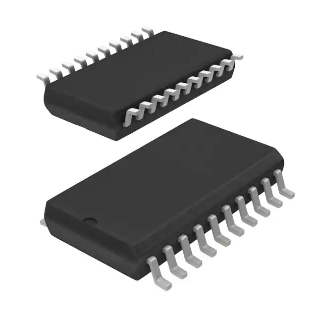
- Part No.:
- U7004B-MFSG3
- Manufacturer:
- Microchip Technology
- Category:
- RF Transceiver ICs
- Package:
- 20-LSSOP (0.173", 4.40mm Width)
- Datasheet:
-
 U7004B-MFSG3.pdf
- Description:
- IC RF TXRX ISM>1GHZ 20SSO
- Quantity:
- Payment:

- Shipping:

Inventory:3,250
Please send an inquiry. Send us your inquiry, and we will respond immediately.
Product details
Overview
U7004B-MFSG3 from Atmel (now Microchip) is a monolithic SiGe transmit/receive front-end IC for DECT 1.88–1.94 GHz TDMA systems, integrating power amplifier (26.5 dBm PSAT), low-noise amplifier (1.8 dB NF), T/R switch driver, and ramp-controlled output power. It operates from a single 3-V supply, supports standby current as low as 10 µA, and eliminates need for external VS switch transistor.
For engineers reviewing the U7004B-MFSG3 datasheet, U7004B-MFSG3 pinout, U7004B-MFSG3 application, or U7004B-MFSG3 equivalent, key selection considerations include its integrated PA+LNA+T/R driver architecture, 20-pin SSO20 package, ramp voltage control interface (0.5–2.0 mA), and DECT-specific timing and burst-mode operation compliance.
Technical Context
The U7004B-MFSG3 implements a fully integrated RF front-end with separate bias paths for PA (pins 6, 10, 13) and LNA (pin 16), internal 50-Ω matching on PA_IN and LNA_IN, and programmable T/R switch current via R_SWITCH resistor. Its ramp-control input (pin 14) enables precise linear output power modulation across 48 dB gain range.
It operates in three defined logic states: Standby (PU=0, RX_ON=0), TX (PU=1, RX_ON=0), and RX (PU=1, RX_ON=1), with quiescent currents of 10 µA (standby), 450 mA (TX), and 8 mA (RX). All RF ports are DC-blocked and require external matching per Figures 13–14.
Key Specifications
| Parameter | Value and Actual Design Meaning |
|---|---|
| Frequency Range | 1.88–1.94 GHz - Matches DECT ETSI EN 300 175 standard band; no external tuning required. |
| Saturated Output Power | 26.5 dBm - Enables +26 dBm peak transmit power into antenna with external matching network. |
| Noise Figure | 1.8 dB typical - Ensures high RX sensitivity in low-SNR DECT handset environments. |
| Power-Added Efficiency | 30% - Reduces thermal load and extends battery life in portable DECT terminals. |
| Ramp Control Current | 0.5–2.0 mA - Directly interfaces with baseband controller's DAC or GPIO for closed-loop power control. |
| Supply Voltage Range | 2.7–4.6 V - Supports wide-input Li-ion battery operation (3.0–4.2 V nominal) without regulation. |
| Standby Current | 10 µA - Meets DECT low-power idle mode requirements for extended standby time. |
Pinout & Package
U7004B-MFSG3 is housed in a 20-pin SSO20 (Small Outline, Shrink) package (6.75 × 6.50 mm, 0.65 mm pitch), lead-free and RoHS-compliant per Atmel documentation.
| Pin/Terminal | Circuit Role | Design Meaning |
|---|---|---|
| 1 R_SWITCH | Resistor bias input | Sets PIN diode current via external resistor to GND; defines T/R switch drive level. |
| 2 SWITCH_OUT | T/R switch current output | Delivers programmable current (up to 10 mA) to external PIN diode for antenna switching. |
| 4 LNA_IN | LNA RF input | 50-Ω matched input for RX path; requires DC blocking capacitor per Figure 8. |
| 10 V2_PA_OUT | PA output matching node | Connects to external inductor and matching network for 50-Ω antenna interface (Figure 13). |
| 14 RAMP | Analog power control input | Voltage-controlled gain setting (0–2.1 V) enabling linear POUT ramping per Figure 3. |
| 15 PA_IN | PA RF input | 50-Ω matched input; accepts up to +10 dBm input; requires DC blocking per Figure 4. |
| 16 VS_LNA | LNA supply | Independent 2.7–4.6 V supply rail; decoupled with 1 µF and 100 pF capacitors (Figure 14). |
| 18 LNA_OUT | LNA RF output | 50-Ω matched output feeding mixer or IF stage; requires DC blocking per Figure 9. |
| 19 RX_ON | Logic enable for RX mode | Active-high control (2.4–VS) selecting LNA path and disabling PA; TTL/CMOS compatible. |
| 20 PU | Global power-up enable | Active-high master enable; must be high for any functional mode (TX/RX); pulls all blocks from standby. |
Key Features
| Feature | Design Value |
|---|---|
| Integrated PA + LNA + T/R driver | Reduces BOM count by eliminating 3 discrete RF blocks and associated matching components. |
| Ramp-controlled output power | Enables compliant DECT burst envelope shaping without external DAC or op-amp circuitry. |
| Single 3-V supply operation | Eliminates need for dual-rail or charge-pump supplies in battery-powered DECT handsets. |
| Ultra-low standby current (10 µA) | Supports >1-week standby on single AA battery without compromising wake-up latency. |
| Internal 50-Ω matching on RF ports | Minimizes layout sensitivity and reduces PCB area vs. discrete matching networks. |
Applications
| DECT Handset Transceiver | DECT Base Station Front-End |
|---|---|
Use Scenario: Full-duplex voice transmission in portable DECT handsets operating in 1.88–1.94 GHz band with 10 ms burst timing. IC Role / Device Role / Timing Role: Single-chip RF front-end handling both TX amplification (26.5 dBm) and RX low-noise reception (1.8 dB NF) with T/R switching. Use Value: Eliminates discrete PA/LNA/Switch design, cuts RF section footprint by >40%, and ensures ETSI-compliant spectral mask via ramp control. | Use Scenario: Multi-channel DECT base station supporting up to 6 simultaneous handsets with full duplex operation. IC Role / Device Role / Timing Role: High-linearity front-end providing stable 26.5 dBm output and 19 dB LNA gain across temperature and supply variation. Use Value: Enables compact multi-channel RF module design with consistent gain flatness and harmonic suppression (<−30 dBc). |
| Wireless Office Phone System | DECT IoT Gateway |
Use Scenario: Low-cost cordless office phone requiring long battery life, clear audio, and interference-resistant 1.9 GHz operation. IC Role / Device Role / Timing Role: Integrated transceiver IC managing burst-mode TX/RX switching, power ramping, and low-noise receive path. Use Value: Achieves >200 hours talk time via 10 µA standby and 30% PAE, while maintaining <2 dB gain variation over −25°C to +70°C. | Use Scenario: Battery-powered DECT-based smart home gateway aggregating sensor data from multiple DECT endpoints. IC Role / Device Role / Timing Role: Low-power front-end enabling periodic beacon transmission and scheduled RX listening windows. Use Value: Supports duty-cycled operation with sub-10 µA deep-sleep current and fast wake-up (<10 µs) via PU/RX_ON control. |
Equivalent & Alternatives
The following parts are listed as comparable options for similar DECT front-end applications.
| Alternative Part | Technical Difference | Application Difference | Selection Advice |
|---|---|---|---|
| RFM69HCW | Sub-GHz (433/868/915 MHz) transceiver; no integrated LNA or T/R driver; requires external PA/LNA matching. | Designed for LoRaWAN/Sigfox, not DECT; lacks ramp control and 1.9 GHz optimization. | Select only for non-DECT ISM-band systems requiring lower data rate and longer range. |
| SKY77557 | 1.9 GHz LTE PA module (no LNA or T/R driver); 5-pin package; requires external LNA and switch. | Targeted at LTE handsets; lacks DECT burst timing support, ramp interface, and standby current optimization. | Use only in LTE infrastructure where DECT compliance and ultra-low standby are not required. |
Compared with RFM69HCW and SKY77557, the U7004B-MFSG3 uniquely integrates PA, LNA, and T/R driver in one 1.9 GHz DECT-optimized die, delivers 26.5 dBm output with 30% PAE, and achieves 10 µA standby-enabling true single-chip DECT handset implementation without compromise.
Availability
U7004B-MFSG3 is available at Aetrix Electronics and suitable for DECT handsets, base stations, wireless office phones, and DECT IoT gateways requiring stable component supply, long-lifecycle support, and RoHS-compliant packaging.
Supply support for U7004B-MFSG3 includes scheduled delivery planning, volume procurement assistance, BOM continuity management, traceable sourcing, and lifecycle availability coordination for OEM customers, industrial embedded developers, connected-device designers, and electronics production programs.
Manufacturer
Atmel Corporation (acquired by Microchip Technology in 2016) is a fabless semiconductor company specializing in microcontrollers, RF ICs, and secure authentication devices.
The U7004B-MFSG3 belongs to Atmel's DECT RF front-end product line, designed specifically for low-power, high-integration 1.88–1.94 GHz TDMA voice and data systems in consumer and enterprise cordless telephony.
FAQ
What is the primary application domain for the U7004B-MFSG3?
The U7004B-MFSG3 is engineered exclusively for DECT (Digital Enhanced Cordless Telecommunications) systems operating in the 1.88–1.94 GHz band. It serves as a complete RF front-end in handsets and base stations, delivering integrated power amplification, low-noise reception, and T/R switching with ramp-controlled output power-fully aligned with ETSI EN 300 175 timing and spectral requirements. The U7004B-MFSG3 does not support LTE, Wi-Fi, or Bluetooth protocols.
Does the U7004B-MFSG3 require external matching components?
Yes, the U7004B-MFSG3 requires external matching networks on PA_IN (pin 15), V2_PA_OUT (pin 10), and LNA_IN (pin 4), as specified in Figures 13 and 14 of the datasheet. While internal 50-Ω matching is provided at these ports, optimal performance-including 26.5 dBm PSAT, <2:1 VSWR, and −30 dBc harmonics-depends on the recommended 2.7 nH inductor, 56 pF capacitors, and microstrip layout. The U7004B-MFSG3 cannot achieve full specification without these external elements.
What is the function of the RAMP pin (pin 14) on the U7004B-MFSG3?
The RAMP pin (pin 14) on the U7004B-MFSG3 is an analog voltage input that linearly controls output power across a 48 dB gain range. Applying 0–2.1 V sets POUT from −20 to +26.5 dBm (per Figure 3), enabling precise DECT-compliant burst envelope shaping. It draws 0.5–2.0 mA and must be driven by a low-impedance source; the U7004B-MFSG3 does not include internal DAC or ramp generator-external baseband control is required.
How does the U7004B-MFSG3 manage power sequencing between TX and RX modes?
The U7004B-MFSG3 uses two dedicated logic inputs-PU (pin 20) and RX_ON (pin 19)-to define three operational states: Standby (PU=0, RX_ON=0), TX (PU=1, RX_ON=0), and RX (PU=1, RX_ON=1). This hardwired control eliminates need for sequencer ICs. During mode transitions, internal biasing ensures no shoot-through current; the U7004B-MFSG3 achieves <10 µs wake-up from standby when PU goes high.
Is the U7004B-MFSG3 pin-compatible with earlier U7004 variants like U7004B-MFS?
Yes, the U7004B-MFSG3 shares identical pinout, electrical behavior, and thermal profile with U7004B-MFS-the only difference is tape-and-reel packaging (G3 suffix) versus tube packaging (no suffix). Both use the same SSO20 footprint, pin assignments, and absolute maximum ratings. No PCB redesign or firmware change is needed when migrating from U7004B-MFS to U7004B-MFSG3.
U7004B-MFSG3 Specifications
- Product attributes
- Attribute value
- Manufacturer:
- Microchip Technology
- Series:
- -
- Package/Case:
- 20-LSSOP (0.173", 4.40mm Width)
- Packaging:
- Tape & Reel (TR)
- Product Status:
- Obsolete
- Programmable:
- Not Verified
- Type:
- TxRx Only
- RF Family/Standard:
- General ISM > 1GHz
- Protocol:
- -
- Modulation:
- -
- Frequency:
- 1.9GHz
- Data Rate (Max):
- -
- Power - Output:
- 26.5dBm
- Sensitivity:
- -
- Memory Size:
- -
- Serial Interfaces:
- -
- GPIO:
- -
- Voltage - Supply:
- 2.7V ~ 4.6V
- Current - Receiving:
- 8mA
- Current - Transmitting:
- 450mA
- Operating Temperature:
- -25°C ~ 70°C
- Grade:
- -
- Qualification:
- -
- Supplier Device Package:
- 20-SSO
U7004B-MFSG3 FAQ
1.How can I place an order for U7004B-MFSG3 through Aetrix?
Please submit a Request for Quotation (RFQ) for U7004B-MFSG3 on Aetrix. Our sales agent will provide a competitive quotation and guide you through the order confirmation once you accept the terms.
2.Are the price and stock information for U7004B-MFSG3 reliable?
The price and inventory of U7004B-MFSG3 are updated periodically and may fluctuate due to market conditions. Stock and pricing data are typically refreshed every 24 hours. Quotation validity for U7004B-MFSG3 is usually 5 days.
3.What payment methods are accepted for U7004B-MFSG3?
We accept Wire Transfer, PayPal, Credit Card, Western Union, MoneyGram, and Escrow for U7004B-MFSG3 transactions.
Note: Certain payment methods may incur a processing fee.
4.How is shipping managed for U7004B-MFSG3?
U7004B-MFSG3 orders can be shipped via leading logistics carriers, including DHL, UPS, FedEx, TNT, or Registered Mail.
Once your U7004B-MFSG3 order is processed, you will receive an email with the shipment details and tracking number.
Note: Tracking information may take up to 24 hours to appear. Express delivery typically takes 3–5 business days.
5.How can I obtain technical support or documentation for U7004B-MFSG3?
For technical support, including U7004B-MFSG3 datasheets, pinout diagrams, or application guidance, please contact our engineering support team. They can provide detailed documentation and assistance for your U7004B-MFSG3 requirements.
6.How does Aetrix verify that U7004B-MFSG3 is sourced from the original manufacturer or authorized distributors?
All U7004B-MFSG3 products on Aetrix are procured from qualified distributors and authorized channels. Our dedicated quality assurance team conducts strict verification, including traceability checks and, if necessary, third-party testing. This ensures that U7004B-MFSG3 meets industry standards.
7.What is the process for return or replacement of U7004B-MFSG3?
All U7004B-MFSG3 units undergo pre-shipment inspection (PSI). If there is an issue with U7004B-MFSG3, returns or replacements are accepted under the following conditions:
1.Quantity discrepancies, incorrect items, or visible external defects (such as breakage or corrosion), acknowledged by Aetrix.
2.The issue is reported within 90 days of delivery.
3.The U7004B-MFSG3 part is unused and in its original packaging.
Return procedure for U7004B-MFSG3:
1.Submit a request within 90 days.
2.Obtain a Return Material Authorization (RMA) from Aetrix.
U7004B-MFSG3 Tags

-
ESP32-D0WD-V3
Espressif Systems

-
ESP8266EX
Espressif Systems

-
ESP32-S3
Espressif Systems

-
NRF24L01P-R7
Nordic Semiconductor ASA
-
NRF24L01P-R
Nordic Semiconductor ASA

-
ESP32-U4WDH
Espressif Systems

-
DA14531-00000OG2
Renesas
-
ESP32-C6FH4
Espressif Systems

-
DA14531-00000FX2
Renesas
-
NRF24L01P-T
Nordic Semiconductor ASA

-
NRF52810-QCAA-R
Nordic Semiconductor ASA
-
ESP32-S3FN8
Espressif Systems
Tech Hub

TTL and CMOS logic families differ in thresholds, loading, output drive, power and timing. This engineering guide compares 74HC and 74HCT, calculates noise margins and checks 3.3 V/5 V compatibility.

A practical engineering guide to 3.3V and 5V logic compatibility, input thresholds, resistor dividers, translator ICs, MOSFET level shifting, I2C pull-ups, timing limits and power-sequencing risks.

The 74HC595 uses push-pull logic outputs, while the TPIC6B595 uses 50 V open-drain DMOS sinks for higher-power loads. This guide compares timing, current limits, 3.3 V interfacing, load wiring, thermal…

The 74HC595 converts serial data into eight stable parallel outputs. This guide covers pin functions, shift and storage timing, OE and MR behavior, drive-current limits, cascading, voltage compatibilit…

A technical comparison of level-sensitive latches and edge-triggered flip-flops, covering timing windows, setup and hold limits, master–slave operation, time borrowing, race-through, HDL inference and…

A D latch stores one bit while Enable controls when data can pass. This reference covers gate-level operation, truth tables, transparency, setup and hold timing, LE versus OE, common ICs and practical …

An SR latch stores one bit through cross-coupled feedback. This engineering reference covers NOR and NAND implementations, truth tables, forbidden-state recovery, gated operation, switch debouncing, fa…

Latch circuits retain one bit through feedback. This technical reference covers SR and D latches, truth tables, transparency, timing limits, latch-versus-flip-flop behavior, applications and common log…

An engineering guide to LED driver operation, constant-current and constant-voltage outputs, linear and switching topologies, dimming, IC selection, calculations, replacement compatibility, and fault c…

Operational amplifier guide covering op amp basics, feedback, ideal vs real op amps, common configurations, buffer circuits, offset, bias current, gain-bandwidth, slew rate, rail-to-rail limits and sel…


