
 My Inquiry
 My Account


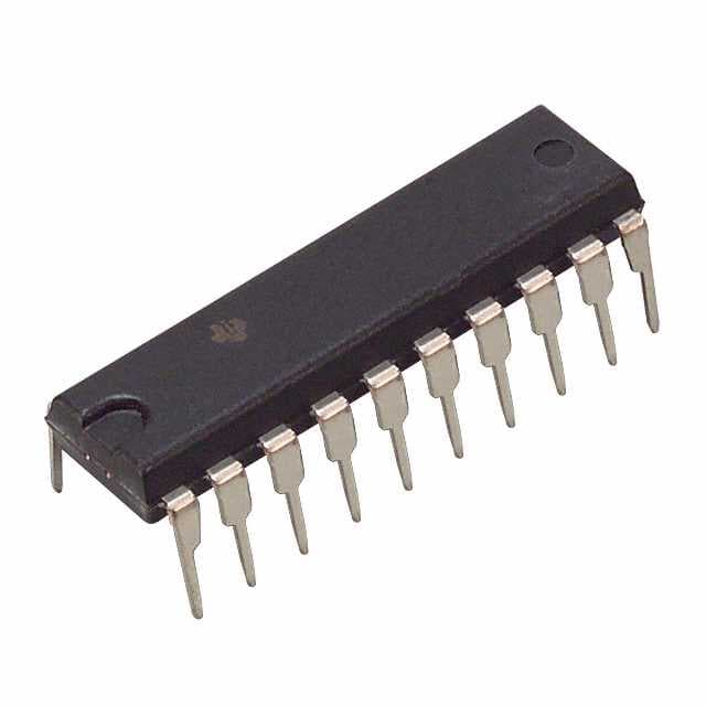
Texas Instruments UCC28503N
- Part No.:
- UCC28503N
- Manufacturer:
- Texas Instruments
- Category:
- PFC (Power Factor Correction)
- Package:
- 20-DIP (0.300", 7.62mm)
- Datasheet:
-
 UCC28503N.pdf
- Description:
- IC PFC CTR AV CURR 120KHZ 20DIP
- Quantity:
- Payment:

- Shipping:

Inventory:2,481
Please send an inquiry. Send us your inquiry, and we will respond immediately.
Product details
Overview
UCC28503N from Texas Instruments is a dual-stage active power factor correction (PFC) and DC-DC controller IC for off-line AC-DC power supplies. It integrates average-current-mode PFC control with peak-current-mode downstream PWM, supports 85–265 VRMS universal input, delivers near-unity power factor, features programmable 80–120 kHz oscillator, and implements synchronized leading-edge (PFC) / trailing-edge (DC-DC) modulation to minimize bulk capacitor ripple in 100-W boost-forward topologies.
For engineers reviewing the UCC28503N datasheet, UCC28503N pinout, UCC28503N application, or UCC28503N equivalent, key selection criteria include its narrow UVLO threshold (10.5 V turn-on / 10 V turn-off), 50% max duty cycle clamp on GT2, VERR-based secondary-side error feedback, and dedicated PFC overvoltage/enable (OVP/ENBL) and zero-power detection (0.33 V VAOUT threshold) functions.
Technical Context
The UCC28503N implements a two-stage control architecture: the PFC stage uses average current-mode control with line-voltage feedforward (VFF) derived from IAC mirroring and a single-pole external filter, enabling constant input power across 3:1 input voltage range; the second stage employs peak-current-mode control with externally generated error signal fed via VERR and internal slope compensation via ISENSE2.
Its UVLO2 threshold is configured for wide-range operation (6.75 V turn-on ±0.75 V hysteresis), allowing second-stage activation down to 50% of nominal bulk voltage-distinct from UCC28501's 75% limit-and it enforces synchronized soft-start sequencing: PFC must reach regulation before SS2 charges and enables GT2, preventing overstress during startup.
Key Specifications
| Parameter | Value and Actual Design Meaning |
|---|---|
| UVLO Threshold | 10.5 V turn-on / 10 V turn-off (narrow hysteresis, optimized for fixed bias supply) |
| Oscillator Frequency | 80–120 kHz (programmable via RT/CT; 100 kHz typical at RT=22 kΩ, CT=330 pF) |
| PFC Gate Driver (GT1) | 95% max duty cycle; 5–12 Ω pull-up/pull-down resistance; 25–50 ns rise/fall time (1 nF load) |
| DC-DC Gate Driver (GT2) | 50% max duty cycle clamp; 5–12 Ω pull-up/pull-down; 25–50 ns rise/fall time (1 nF load) |
| Voltage Reference (VREF) | 7.5 V ±15 mV (–40°C to 85°C); 10 mA sink capability; disabled below UVLO |
| Zero-Power Detection | 0.33 V VAOUT threshold (0.175–0.5 V range); disables output when bulk voltage collapses |
| Second-Stage Enable Threshold | OVP/ENBL pin: 1.9 V enables both stages; <1.7 V disables PFC & DC-DC and resets SS2 |
Pinout & Package
UCC28503N is supplied in a 20-pin plastic DIP (N) package with 0.3-inch body width and through-hole mounting. Thermal performance is rated for –40°C to 85°C ambient operation; power dissipation limited to 1 W.
| Pin/Terminal | Circuit Role | Design Meaning |
|---|---|---|
| GT1 | PFC gate driver output | Totem-pole MOSFET driver for boost switch; supports 95% max duty cycle and fast switching (25–50 ns) |
| GT2 | DC-DC gate driver output | Totem-pole driver for forward/Flyback switch; internally clamped to ≤50% duty cycle for safe transformer reset |
| IAC | AC line current sensing input | Current-input pin feeding analog multiplier; mirrored to VFF for RMS feedforward; max 500 µA |
| VFF | RMS feedforward voltage node | Generated by IAC mirroring + external RC filter; sets 1.4 V (low line) to 4.7 V (high line) scaling for constant power |
| VAOUT | PFC voltage amplifier output | Regulates boost output voltage; internally clamped to ~5.5 V; zero-power comparator input (0.33 V threshold) |
| VERR | DC-DC error amplifier input | Receives opto-coupled secondary-side error signal; 4.5 V internal clamp limits GT2 duty cycle to <50% |
| OVP/ENBL | Window comparator enable | Disables PFC if boost exceeds +6.67%; disables both stages if pulled <1.9 V; defines active range for DC-DC |
| SS2 | DC-DC soft-start control | Charges external capacitor with –10 µA current; held low until PFC reaches regulation; discharges rapidly on fault |
| PKLMT | PFC peak current limit threshold | 0 V reference; requires resistor divider from current-sense resistor negative terminal to VREF for level-shifting |
| VSENSE | PFC voltage feedback input | Inverting input of voltage error amp; connected to resistive divider from boost output; used with VAOUT for loop compensation |
Key Features
| Feature | Design Value |
|---|---|
| Synchronized dual-stage modulation | Leading-edge PFC + trailing-edge DC-DC reduces overlap conduction, cutting bulk capacitor ripple current by >30% vs unsynchronized designs |
| Integrated line feedforward (VFF) | IAC mirroring + single-pole RC eliminates high-voltage dividers and reduces component count while maintaining ±1% input power regulation |
| Programmable soft-start sequencing | Internal logic prevents GT2 activation until VAOUT ≥90% of target; SS2 ramps linearly only after PFC stabilization |
| Dedicated zero-power detection | 0.33 V VAOUT comparator shuts down GT1/GT2 when bulk voltage collapses, preventing uncontrolled restarts during brownouts |
| Wide UVLO2 operating range | 6.75 V turn-on with 3 V hysteresis allows DC-DC operation down to 50% of nominal bulk voltage-critical for holdup extension |
Applications
| Industrial AC-DC Power Supplies | Medical Equipment Power Modules |
|---|---|
Use Scenario: 100-W universal-input (85–265 VRMS) offline power supply for PLC controllers with 16-ms holdup requirement. IC Role / Device Role / Timing Role: UCC28503N performs PFC pre-regulation (boost) and isolated DC-DC conversion (forward topology) with synchronized timing to minimize output capacitor stress. Use Value: Reduces bulk capacitor ripple current by 35%, enabling use of smaller 100 µF/450 V electrolytic instead of 220 µF, lowering BOM cost and footprint. | Use Scenario: Compact, low-noise 12-V/8.3-A power module for portable ultrasound imaging systems requiring Class I safety and low EMI. IC Role / Device Role / Timing Role: UCC28503N controls continuous-conduction-mode boost PFC and transformer-isolated forward converter, with VERR-fed opto feedback ensuring tight secondary-side regulation. Use Value: Zero-power detection (0.33 V VAOUT) ensures immediate shutdown during AC dropout, meeting IEC 60601-1 "loss of mains" safety response requirements. |
| LED Driver Front-Ends | Server PSU Auxiliary Rails |
Use Scenario: 150-W constant-voltage LED driver for outdoor signage operating across global AC grids with THD <10%. IC Role / Device Role / Timing Role: UCC28503N shapes input current using average-current-mode PFC and regulates intermediate 385-V bus before buck-derived LED current control. Use Value: Programmable 100-kHz oscillator enables EMI spread-spectrum tuning; VFF feedforward maintains <±2% input power variation over full line range. | Use Scenario: Auxiliary 5-V/3-A rail in 1U server PSU supporting always-on management controllers during main rail brownout. IC Role / Device Role / Timing Role: UCC28503N powers auxiliary converter from boosted bus; UVLO2 wide hysteresis (3 V) sustains operation down to 192 V bulk (50% of 385 V). Use Value: Enables 16-ms holdup at full load without additional energy storage, reducing reliance on large holdup capacitors in space-constrained 1U chassis. |
Equivalent & Alternatives
The following parts are listed as comparable options for similar dual-stage PFC + DC-DC controller applications.
| Alternative Part | Technical Difference | Application Difference | Selection Advice |
|---|---|---|---|
| UCC28501N | Narrow UVLO (10.5 V/10 V) but narrower UVLO2 hysteresis (1.2 V); supports only down to 75% bulk voltage | Less suitable for extended holdup designs requiring operation below 289 V (75% of 385 V) | Select UCC28501N only when strict 75% minimum bulk voltage is acceptable and cost-sensitive biasing is needed |
| UCC28503DW | Identical electrical specs and pinout; SOIC-20 (DW) package instead of PDIP-20 (N) | Requires PCB redesign for surface-mount assembly; better thermal performance at high density | Choose UCC28503DW for automated SMT production or improved thermal management; no circuit changes needed |
Compared with UCC28501N, UCC28503N provides wider UVLO2 hysteresis (3.0 V vs. 1.2 V) enabling reliable operation down to 50% bulk voltage-critical for long holdup-while UCC28503DW offers identical functionality in a space-efficient SOIC package for volume manufacturing.
Availability
UCC28503N is available at Aetrix Electronics and suitable for industrial AC-DC power supplies, medical equipment power modules, LED driver front-ends, and server PSU auxiliary rails requiring stable component supply, long-term lifecycle support, and traceable sourcing.
Supply support for UCC28503N includes scheduled delivery planning, volume procurement assistance, BOM continuity management, traceable sourcing, and lifecycle availability coordination for OEM customers, industrial embedded developers, connected-device designers, and electronics production programs.
Manufacturer
Texas Instruments is a global semiconductor company headquartered in Dallas, Texas, delivering analog and embedded processing solutions for industrial, automotive, and communications markets.
The UCC2850x product line was engineered specifically for cost-sensitive, high-efficiency two-stage AC-DC conversion in universal-input offline power supplies, integrating PFC and DC-DC control to eliminate discrete controller duplication and reduce system-level component count.
FAQ
What is the UVLO behavior of the UCC28503N and how does it differ from other UCC2850x variants?
The UCC28503N features a narrow VCC UVLO threshold of 10.5 V turn-on / 10 V turn-off, optimized for fixed-bias operation. Its second-stage UVLO2 has a 3.0 V hysteresis (6.75 V turn-on), enabling operation down to 50% of nominal bulk voltage-unlike UCC28501N's 1.2 V hysteresis and 75% limit. This makes UCC28503N uniquely suited for extended holdup applications where sustained DC-DC operation during brownouts is required. All specifications are confirmed in the SLUS419C datasheet absolute maximum and electrical characteristics tables.
How does the UCC28503N implement synchronized start-up between the PFC and DC-DC stages?
The UCC28503N enforces strict sequencing: the PFC stage must first regulate the boost output (detected via VAOUT reaching ~90% of target) before the SS2 pin begins charging. Only then does the DC-DC stage activate via GT2. If VAOUT drops below the zero-power threshold (0.33 V), both GT1 and GT2 shut down immediately. This prevents the DC-DC stage from drawing excessive current before the PFC bus is stable-a critical reliability feature documented in the SLUS419C Typical Application section and block diagram.
What is the function of the VFF pin on the UCC28503N and how is it implemented externally?
The VFF pin on the UCC28503N carries the RMS feedforward voltage generated by mirroring half the IAC current into an external RC low-pass filter. With IAC = 150 µA at low line, VFF ≈ 1.4 V; at high line (IAC = 500 µA), VFF ≈ 4.7 V. This scaling ensures constant input power across 85–265 VRMS input without high-voltage resistors. The SLUS419C datasheet Figure 3 and Pin Assignments section confirm this implementation and specify recommended R/C values for 120-Hz ripple attenuation.
Can the UCC28503N support both voltage-mode and current-mode control for the DC-DC stage?
Yes-the UCC28503N supports both modes. For current-mode control, the external error signal is applied to VERR, and the ISENSE2 pin receives the current-sense signal plus optional slope compensation from the CT ramp. For voltage-mode control, the CT ramp is fed back into ISENSE2 via a voltage divider, eliminating the need for a separate ramp generator. This dual-mode flexibility is explicitly described in the SLUS419C Typical Application section on page 12 and verified in the block diagram (page 8).
What are the absolute maximum ratings for gate drive current and supply voltage on the UCC28503N?
The UCC28503N specifies 1.2 A pulsed gate drive current per output (GT1 or GT2) and 0.2 A continuous drive current, with VCC absolute maximum rating of 18 V. Exceeding 18 V risks permanent damage, and operation above 17 V is outside recommended conditions. These values are listed in the Absolute Maximum Ratings table (page 2) of SLUS419C and validated across all UCC2850x variants regardless of UVLO configuration.
UCC28503N Specifications
- Product attributes
- Attribute value
- Manufacturer:
- Texas Instruments
- Series:
- -
- Package/Case:
- 20-DIP (0.300", 7.62mm)
- Packaging:
- Tube
- Product Status:
- Obsolete
- Mode:
- Average Current
- Frequency - Switching:
- 80kHz ~ 120kHz
- Current - Startup:
- 150 µA
- Voltage - Supply:
- 9.7V ~ 18V
- Operating Temperature:
- -40°C ~ 85°C
- Grade:
- -
- Qualification:
- -
- Mounting Type:
- Through Hole
- Supplier Device Package:
- 20-PDIP
UCC28503N FAQ
1.How can I place an order for UCC28503N through Aetrix?
Please submit a Request for Quotation (RFQ) for UCC28503N on Aetrix. Our sales agent will provide a competitive quotation and guide you through the order confirmation once you accept the terms.
2.Are the price and stock information for UCC28503N reliable?
The price and inventory of UCC28503N are updated periodically and may fluctuate due to market conditions. Stock and pricing data are typically refreshed every 24 hours. Quotation validity for UCC28503N is usually 5 days.
3.What payment methods are accepted for UCC28503N?
We accept Wire Transfer, PayPal, Credit Card, Western Union, MoneyGram, and Escrow for UCC28503N transactions.
Note: Certain payment methods may incur a processing fee.
4.How is shipping managed for UCC28503N?
UCC28503N orders can be shipped via leading logistics carriers, including DHL, UPS, FedEx, TNT, or Registered Mail.
Once your UCC28503N order is processed, you will receive an email with the shipment details and tracking number.
Note: Tracking information may take up to 24 hours to appear. Express delivery typically takes 3–5 business days.
5.How can I obtain technical support or documentation for UCC28503N?
For technical support, including UCC28503N datasheets, pinout diagrams, or application guidance, please contact our engineering support team. They can provide detailed documentation and assistance for your UCC28503N requirements.
6.How does Aetrix verify that UCC28503N is sourced from the original manufacturer or authorized distributors?
All UCC28503N products on Aetrix are procured from qualified distributors and authorized channels. Our dedicated quality assurance team conducts strict verification, including traceability checks and, if necessary, third-party testing. This ensures that UCC28503N meets industry standards.
7.What is the process for return or replacement of UCC28503N?
All UCC28503N units undergo pre-shipment inspection (PSI). If there is an issue with UCC28503N, returns or replacements are accepted under the following conditions:
1.Quantity discrepancies, incorrect items, or visible external defects (such as breakage or corrosion), acknowledged by Aetrix.
2.The issue is reported within 90 days of delivery.
3.The UCC28503N part is unused and in its original packaging.
Return procedure for UCC28503N:
1.Submit a request within 90 days.
2.Obtain a Return Material Authorization (RMA) from Aetrix.
UCC28503N Tags

-
ICE2PCS01GXUMA1
Infineon Technologies

-
NCP1654BD133R2G
onsemi
-
MC33262DR2G
onsemi
-
ICE3PCS03GXUMA1
Infineon Technologies
-
NCP1631DR2G
onsemi

-
L4981BD013TR
STMicroelectronics
-
UCC28070DWR
Texas Instruments

-
UCC28070PWR
Texas Instruments

-
UC3854DWTR
Texas Instruments
-
L4981AD013TR
STMicroelectronics

-
UCC2817D
Texas Instruments
-
UC2854BDWTR
Texas Instruments
Tech Hub

A practical engineering guide to 3.3V and 5V logic compatibility, input thresholds, resistor dividers, translator ICs, MOSFET level shifting, I2C pull-ups, timing limits and power-sequencing risks.

The 74HC595 uses push-pull logic outputs, while the TPIC6B595 uses 50 V open-drain DMOS sinks for higher-power loads. This guide compares timing, current limits, 3.3 V interfacing, load wiring, thermal…

The 74HC595 converts serial data into eight stable parallel outputs. This guide covers pin functions, shift and storage timing, OE and MR behavior, drive-current limits, cascading, voltage compatibilit…

A technical comparison of level-sensitive latches and edge-triggered flip-flops, covering timing windows, setup and hold limits, master–slave operation, time borrowing, race-through, HDL inference and…

A D latch stores one bit while Enable controls when data can pass. This reference covers gate-level operation, truth tables, transparency, setup and hold timing, LE versus OE, common ICs and practical …

An SR latch stores one bit through cross-coupled feedback. This engineering reference covers NOR and NAND implementations, truth tables, forbidden-state recovery, gated operation, switch debouncing, fa…

Latch circuits retain one bit through feedback. This technical reference covers SR and D latches, truth tables, transparency, timing limits, latch-versus-flip-flop behavior, applications and common log…

An engineering guide to LED driver operation, constant-current and constant-voltage outputs, linear and switching topologies, dimming, IC selection, calculations, replacement compatibility, and fault c…

Operational amplifier guide covering op amp basics, feedback, ideal vs real op amps, common configurations, buffer circuits, offset, bias current, gain-bandwidth, slew rate, rail-to-rail limits and sel…

Jumper cables guide covering safe connection order, red and black clamp placement, final ground connection, cable gauge, length, clamp quality, copper vs CCA cables, jump starter comparison and battery…


