
 My Inquiry
 My Account


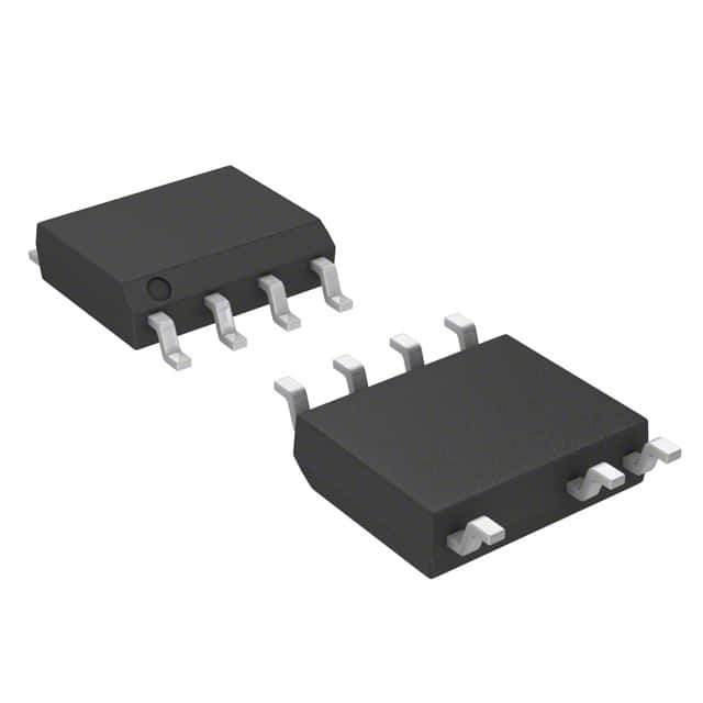
Texas Instruments UCC28711DR
- Part No.:
- UCC28711DR
- Manufacturer:
- Texas Instruments
- Category:
- AC DC Converters, Offline Switches
- Package:
- 8-SOIC (0.154", 3.90mm Width), 7 Leads
- Datasheet:
-
 UCC28711DR.pdf
- Description:
- IC OFFLINE SWITCH FLYBACK 7SOIC
- Quantity:
- Payment:

- Shipping:

Inventory:4,143
Please send an inquiry. Send us your inquiry, and we will respond immediately.
Product details
Overview
UCC28711DR from Texas Instruments is a constant-voltage/constant-current flyback controller with primary-side regulation (PSR), eliminating optocouplers in AC-DC adapters. It delivers ±5% voltage/current regulation across line and load, features a 700-V start-up switch, supports up to 100 kHz switching, and integrates NTC thermistor interface for remote temperature sensing - used in USB-compliant smartphone and tablet chargers.
For engineers reviewing the UCC28711DR datasheet, UCC28711DR pinout, UCC28711DR application, or UCC28711DR equivalent, this page provides verified technical context, real-world PSR design implications, confirmed thermal shutdown behavior at 165°C, and validated alternative options for CC/CV adapter designs requiring fixed cable compensation and temperature-aware protection.
Technical Context
The UCC28711DR operates in discontinuous conduction mode (DCM) with valley-switching to minimize MOSFET turn-on losses and uses combined frequency modulation (FM) and amplitude modulation (AM) of peak primary current to maintain high efficiency across 0–100% load. Its internal 700-V HV pin enables direct connection to rectified bulk voltage, while the NTC pin (Pin 3) provides programmable thermal shutdown via external thermistor with 0.95 V threshold and 105 µA pull-up current.
Primary-side regulation relies on precise sampling of the auxiliary winding voltage at transformer demagnetization end, referenced to a stable 4.05 V VS regulating level (±0.04 V). Line-sense functionality is implemented through VS pin current thresholds - 225 µA run and 80 µA stop - enabling automatic AC input detection without auxiliary bias windings.
Key Specifications
| Parameter | Value and Actual Design Meaning |
|---|---|
| Max switching frequency | 100 kHz - enables compact magnetics and high-power-density USB charger designs |
| VS regulating level | 4.05 V ±0.04 V - sets CV output accuracy; drifts −0.8 mV/°C for temperature compensation |
| NTC shutdown threshold | 0.95 V - triggers fault state when external NTC resistor pulls Pin 3 below threshold |
| Constant-current regulation | 330 mV ±13 mV at CS pin - defines CC setpoint; scaled by transformer turns ratio and RCS |
| Start-up HV rating | 700 V - allows direct connection to rectified AC line without external start-up circuitry |
| UVLO thresholds | VDD turn-on at 21 V, turn-off at 8.1 V - ensures reliable start-up and brownout recovery |
| Thermal shutdown | 165 °C - internal junction protection with automatic restart after cooldown |
Pinout & Package
UCC28711DR is housed in a 7-pin SOIC package (4.91 mm × 3.90 mm body size) with Gull-wing leads, rated for −40°C to +125°C operating junction temperature and 141.5°C/W junction-to-ambient thermal resistance.
| Pin/Terminal | Circuit Role | Design Meaning |
|---|---|---|
| VDD (Pin 1) | Bias supply input | Accepts 9–35 V; powers internal circuitry; UVLO window (8.1 V / 21 V) ensures robust start-up and hold-up |
| VS (Pin 2) | Voltage sense input | Connects to auxiliary winding divider; samples output voltage timing and magnitude; also senses AC line for run/stop control |
| NTC (Pin 3) | Temperature sense input | Interface for external NTC thermistor; 105 µA pull-up current creates voltage divider; <0.95 V forces shutdown |
| GND (Pin 4) | Analog and power ground | Common reference for CS, VS, DRV, and internal regulators; requires low-inductance layout near bypass capacitor |
| HV (Pin 7) | High-voltage start-up input | 700-V rated; draws 100–500 µA during start-up to charge VDD capacitor from bulk rail |
| DRV (Pin 6) | MOSFET gate driver output | Clamped 14 V drive; 25 mA source / 10 mA sink capability; RDRVLS = 190 kΩ in start state limits initial gate current |
| CS (Pin 5) | Current sense input | Monitors primary peak current via ground-referenced RCS; 780 mV max threshold; includes 235 ns leading-edge blanking |
Key Features
| Feature | Design Value |
|---|---|
| Primary-side regulation (PSR) | Eliminates optocoupler and secondary-side TL431, reducing BOM count and improving reliability in isolated USB adapters |
| Resonant valley-switching | Reduces MOSFET turn-on loss by triggering gate drive at drain voltage minima, directly improving full-load efficiency |
| Programmable thermal shutdown | NTC interface enables system-level overtemperature protection without additional ICs - critical for enclosed smartphone charger designs |
| Fixed cable compensation | UCC28711DR provides 0-mV compensation at 5-V output, maintaining USB voltage spec under load without external DAC or MCU |
| <10-mW no-load power | Achieved via dynamic state control and low IWAIT (120 µA), meeting Energy Star and EU CoC Tier 2 standby requirements |
Applications
| Smartphone USB Charging Adapter | Tablet Fast-Charging Supply |
|---|---|
|
Use Scenario: Wall adapter delivering 5 V / 2 A to smartphones with tight USB voltage tolerance (4.75–5.25 V) and thermal constraints in plastic enclosures. IC Role / Device Role / Timing Role: PSR controller managing DCM flyback operation, sampling auxiliary winding at demagnetization zero-crossing to regulate output without optocoupler feedback. Use Value: NTC interface enables real-time thermal derating before PCB hotspots exceed 85°C; fixed 0-mV cable compensation maintains 5.0 V ±2% at connector under full load. |
Use Scenario: 12 W tablet charger requiring fast transient response to pulsed load profiles and compliance with USB BC1.2 charging handshaking. IC Role / Device Role / Timing Role: Dual-mode CV/CC regulator using FM+AM control law to sustain regulation from 0.5 A to 2.4 A while maintaining <10-mW standby. Use Value: Valley-switching reduces EMI at fundamental frequency, easing Class B conducted emissions; 100 kHz max fSW allows use of low-cost 650 V GaN or Si MOSFETs. |
| White Goods Standby Power | USB-C PD Auxiliary Bias Supply |
|
Use Scenario: Always-on 5 V / 100 mA auxiliary rail in washing machines or refrigerators, operating continuously across −25°C to +70°C ambient. IC Role / Device Role / Timing Role: Low-power PSR controller using HV pin for direct bulk start-up and wide VDD range (9–35 V) to tolerate brownouts. Use Value: −40°C to +125°C junction rating and 165°C thermal shutdown ensure long-term reliability; 141.5°C/W θJA supports natural convection cooling on FR-4. |
Use Scenario: Secondary 5 V bias supply in multi-output USB-C PD designs, powering microcontroller and communication ICs independent of main PD controller. IC Role / Device Role / Timing Role: Isolated CV regulator with PSR feedback, decoupled from main PD negotiation loop to avoid interference during voltage transitions. Use Value: No optocoupler simplifies safety isolation; SOIC-7 footprint allows placement on secondary-side PCB layer; 700-V HV pin eliminates start-up resistor network. |
Equivalent & Alternatives
The following parts are listed as comparable options for similar constant-voltage/constant-current flyback controller applications.
| Alternative Part | Technical Difference | Application Difference | Selection Advice |
|---|---|---|---|
| UCC28712DR | Provides 150-mV fixed cable compensation at 5-V output vs. UCC28711DR's 0-mV; identical NTC interface and pinout | Suitable for longer cables (e.g., laptop adapters) where voltage drop exceeds USB spec without compensation | Select UCC28712DR when output cable length >1.2 m and full-load regulation must stay within 5.0 V ±2% |
| UCC28713DR | Offers 300-mV fixed cable compensation at 5-V output; same NTC threshold (0.95 V) and thermal shutdown (165°C) | Targeted at high-current USB-C accessories with 3 A loads and >2 m cables requiring aggressive IR drop correction | Choose UCC28713DR only if measured connector voltage drops >250 mV at full load - avoids overcompensation in short-cable applications |
Compared with UCC28711DR, UCC28712DR and UCC28713DR share identical PSR architecture, NTC interface, and SOIC-7 packaging but differ solely in factory-trimmed cable compensation levels - making them non-interchangeable without revalidating output voltage regulation across temperature and load.
Availability
UCC28711DR is available at Aetrix Electronics and suitable for USB-compliant smartphone adapters, tablet fast-charging supplies, and white goods standby power systems requiring stable component supply, long-lifecycle support, and TI-qualified manufacturing traceability.
Supply support for UCC28711DR includes scheduled delivery planning, volume procurement assistance, BOM continuity management, traceable sourcing, and lifecycle availability coordination for OEM customers, industrial embedded developers, connected-device designers, and electronics production programs.
Manufacturer
Texas Instruments is a global semiconductor company specializing in analog and embedded processing technologies, with leadership in power management ICs for consumer, industrial, and automotive markets.
The UCC2871x product line was designed specifically for cost-sensitive, high-efficiency AC-DC flyback converters in USB charging and auxiliary power applications - emphasizing primary-side regulation, ultra-low standby power, and integrated protection.
FAQ
What is the function of the NTC pin on the UCC28711DR?
The NTC pin (Pin 3) on the UCC28711DR interfaces with an external negative temperature coefficient thermistor to enable programmable thermal shutdown. It features a 105 µA internal pull-up current and triggers fault mode when the pin voltage falls below 0.95 V - corresponding to a ~9.05 kΩ thermistor resistance at 25°C. This function is exclusive to UCC28711DR, UCC28712DR, and UCC28713DR; the UCC28710DR lacks this pin entirely. The UCC28711DR uses this feature to protect enclosed USB adapters from overheating during sustained high-load operation.
Does the UCC28711DR support programmable cable compensation like the UCC28710DR?
No, the UCC28711DR does not support programmable cable compensation. Unlike the UCC28710DR - which uses the CBC pin to set compensation via external resistor - the UCC28711DR replaces CBC with the NTC pin and implements fixed 0-mV cable compensation at 5-V output. This is confirmed in the Device Comparison Table and Pin Functions section of the SLUSB86C datasheet. Designers requiring adjustable compensation must select UCC28710DR; those needing thermal monitoring with fixed compensation should use UCC28711DR, UCC28712DR, or UCC28713DR.
What is the maximum switching frequency of the UCC28711DR and how is it controlled?
The UCC28711DR has a maximum switching frequency of 100 kHz, specified at VS = 3.7 V and tested across −40°C to +125°C junction temperature. Frequency is dynamically modulated based on load and line conditions using a combination of frequency modulation (FM) and amplitude modulation (AM) of the primary peak current. The minimum switching frequency is 680 Hz (at VS = 4.35 V), enabling ultra-low standby power. This dual-modulation scheme is intrinsic to the UCC28711DR control law and requires no external programming components.
How does the UCC28711DR achieve primary-side regulation without an optocoupler?
The UCC28711DR achieves primary-side regulation by sampling the voltage on the auxiliary winding at the precise moment of transformer demagnetization completion - detected via the VS pin waveform zero-crossing. This sampled voltage correlates directly to the secondary output voltage, scaled by the auxiliary-to-secondary turns ratio. The internal 4.05 V VS regulating level serves as the CV reference, while the CS pin monitors primary current to enforce CC mode. This eliminates optocoupler latency and aging effects, and is validated across line (85–265 VAC) and load (0–100%) with ±5% total regulation error - a core specification of the UCC28711DR.
What protection features are integrated into the UCC28711DR?
The UCC28711DR integrates six hardware-based protection functions: output overvoltage (VOVP = 4.6 V at VS pin), primary overcurrent (VOCP = 1.5 V at CS pin), AC input undervoltage lockout (IVSL(stop) = 80 µA), internal overtemperature shutdown (TJ = 165°C), CS pin fault detection, and VS pin fault detection. All protections force the device into fault state with IFAULT ≈ 120 µA supply current, discharging VDD until UVLO turnoff (8.1 V), then restarting automatically. These are hard-wired features of the UCC28711DR silicon - no configuration registers or firmware required.
UCC28711DR Specifications
- Product attributes
- Attribute value
- Manufacturer:
- Texas Instruments
- Series:
- -
- Package/Case:
- 8-SOIC (0.154", 3.90mm Width), 7 Leads
- Packaging:
- Tape & Reel (TR)
- Product Status:
- Active
- Output Isolation:
- Isolated
- Internal Switch(s):
- No
- Voltage - Breakdown:
- -
- Topology:
- Flyback
- Voltage - Start Up:
- 21 V
- Voltage - Supply (Vcc/Vdd):
- 9V ~ 35V
- Duty Cycle:
- -
- Frequency - Switching:
- 680Hz ~ 100kHz
- Power (Watts):
- -
- Fault Protection:
- Current Limiting, Over Voltage
- Control Features:
- -
- Operating Temperature:
- -40°C ~ 125°C (TJ)
- Grade:
- -
- Qualification:
- -
- Supplier Device Package:
- 7-SOIC
- Mounting Type:
- Surface Mount
UCC28711DR FAQ
1.How can I place an order for UCC28711DR through Aetrix?
Please submit a Request for Quotation (RFQ) for UCC28711DR on Aetrix. Our sales agent will provide a competitive quotation and guide you through the order confirmation once you accept the terms.
2.Are the price and stock information for UCC28711DR reliable?
The price and inventory of UCC28711DR are updated periodically and may fluctuate due to market conditions. Stock and pricing data are typically refreshed every 24 hours. Quotation validity for UCC28711DR is usually 5 days.
3.What payment methods are accepted for UCC28711DR?
We accept Wire Transfer, PayPal, Credit Card, Western Union, MoneyGram, and Escrow for UCC28711DR transactions.
Note: Certain payment methods may incur a processing fee.
4.How is shipping managed for UCC28711DR?
UCC28711DR orders can be shipped via leading logistics carriers, including DHL, UPS, FedEx, TNT, or Registered Mail.
Once your UCC28711DR order is processed, you will receive an email with the shipment details and tracking number.
Note: Tracking information may take up to 24 hours to appear. Express delivery typically takes 3–5 business days.
5.How can I obtain technical support or documentation for UCC28711DR?
For technical support, including UCC28711DR datasheets, pinout diagrams, or application guidance, please contact our engineering support team. They can provide detailed documentation and assistance for your UCC28711DR requirements.
6.How does Aetrix verify that UCC28711DR is sourced from the original manufacturer or authorized distributors?
All UCC28711DR products on Aetrix are procured from qualified distributors and authorized channels. Our dedicated quality assurance team conducts strict verification, including traceability checks and, if necessary, third-party testing. This ensures that UCC28711DR meets industry standards.
7.What is the process for return or replacement of UCC28711DR?
All UCC28711DR units undergo pre-shipment inspection (PSI). If there is an issue with UCC28711DR, returns or replacements are accepted under the following conditions:
1.Quantity discrepancies, incorrect items, or visible external defects (such as breakage or corrosion), acknowledged by Aetrix.
2.The issue is reported within 90 days of delivery.
3.The UCC28711DR part is unused and in its original packaging.
Return procedure for UCC28711DR:
1.Submit a request within 90 days.
2.Obtain a Return Material Authorization (RMA) from Aetrix.
UCC28711DR Tags
-
LNK6407D-TL
Power Integrations
-
LNK3204D-TL
Power Integrations

-
SR10LG-G
Microchip Technology
-
TNY285DG-TL
Power Integrations
-
LNK304DN-TL
Power Integrations
-
TNY285KG-TL
Power Integrations
-
LNK3206D-TL
Power Integrations
-
LNK623DG-TL
Power Integrations
-
TNY286PG
Power Integrations
-
LNK624DG-TL
Power Integrations
-
LNK604DG-TL
Power Integrations

-
UCC28704DBVR-1
Texas Instruments
Tech Hub

A practical engineering guide to 3.3V and 5V logic compatibility, input thresholds, resistor dividers, translator ICs, MOSFET level shifting, I2C pull-ups, timing limits and power-sequencing risks.

The 74HC595 uses push-pull logic outputs, while the TPIC6B595 uses 50 V open-drain DMOS sinks for higher-power loads. This guide compares timing, current limits, 3.3 V interfacing, load wiring, thermal…

The 74HC595 converts serial data into eight stable parallel outputs. This guide covers pin functions, shift and storage timing, OE and MR behavior, drive-current limits, cascading, voltage compatibilit…

A technical comparison of level-sensitive latches and edge-triggered flip-flops, covering timing windows, setup and hold limits, master–slave operation, time borrowing, race-through, HDL inference and…

A D latch stores one bit while Enable controls when data can pass. This reference covers gate-level operation, truth tables, transparency, setup and hold timing, LE versus OE, common ICs and practical …

An SR latch stores one bit through cross-coupled feedback. This engineering reference covers NOR and NAND implementations, truth tables, forbidden-state recovery, gated operation, switch debouncing, fa…

Latch circuits retain one bit through feedback. This technical reference covers SR and D latches, truth tables, transparency, timing limits, latch-versus-flip-flop behavior, applications and common log…

An engineering guide to LED driver operation, constant-current and constant-voltage outputs, linear and switching topologies, dimming, IC selection, calculations, replacement compatibility, and fault c…

Operational amplifier guide covering op amp basics, feedback, ideal vs real op amps, common configurations, buffer circuits, offset, bias current, gain-bandwidth, slew rate, rail-to-rail limits and sel…

Jumper cables guide covering safe connection order, red and black clamp placement, final ground connection, cable gauge, length, clamp quality, copper vs CCA cables, jump starter comparison and battery…


