
 My Inquiry
 My Account


Texas Instruments UCC3626DWTR
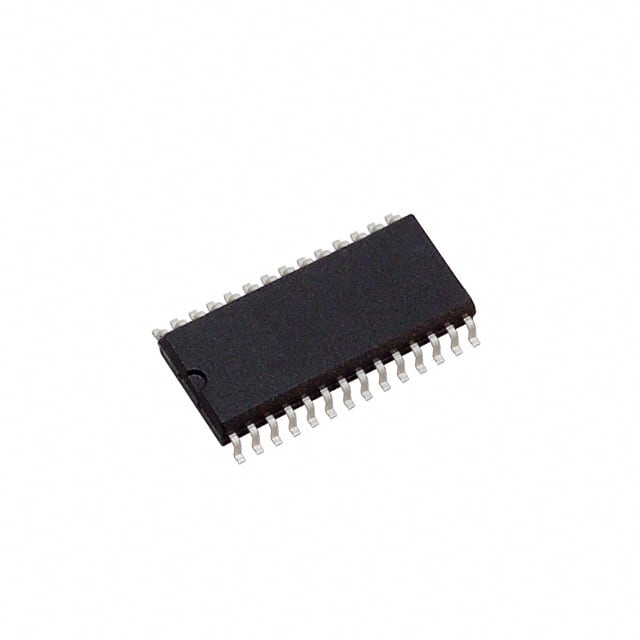
- Part No.:
- UCC3626DWTR
- Manufacturer:
- Texas Instruments
- Category:
- Motor Drivers, Controllers
- Package:
- 28-SOIC (0.295", 7.50mm Width)
- Datasheet:
-
 UCC3626DWTR.pdf
- Description:
- IC MOTOR DRIVER 11V-14.5V 28SOIC
- Quantity:
- Payment:

- Shipping:

Inventory:3,054
Please send an inquiry. Send us your inquiry, and we will respond immediately.
Product details
Overview
UCC3626DWTR from Texas Instruments is a three-phase brushless DC motor controller IC supporting two- and four-quadrant operation, featuring integrated current-sense amplifier (gain = 5 V/V), precision tachometer output (variable duty-cycle, frequency-proportional), and 10 kHz oscillator (RTACH = 250 kΩ, CT = 1 nF). It decodes Hall sensor inputs (HALLA/B/C) to drive six gate outputs (AHI/ALOW/BHI/BLOW/CHI/CLOW) for external power stages in industrial motion control systems.
For engineers reviewing the UCC3626DWTR datasheet, UCC3626DWTR pinout, UCC3626DWTR application, or UCC3626DWTR equivalent, key selection criteria include Hall-based commutation logic, QUAD-selectable PWM modulation mode (low-side only vs. high-/low-side), absolute-value current reconstruction for pulse-by-pulse overcurrent protection, and tachometer timing programmability via R_TACH and C_TACH.
Technical Context
The UCC3626DWTR implements a Hall decoder with direction detection (DIR_IN/DIR_OUT), latched PWM comparator with programmable oscillator (CT pin, triangle waveform), and differential current-sense amplifier with absolute-value output (IOUT = |SNS_I − SNS_NI| × 5). Its oscillator supports synchronization via SYNCH input when paired with matching R_TACH parallel resistor.
Four-quadrant operation (QUAD = 1) enables simultaneous high- and low-side PWM modulation for controlled torque reversal and continuous current sensing; two-quadrant mode (QUAD = 0) modulates only low-side switches, reducing switching losses but limiting braking capability without external diode routing.
Key Specifications
| Parameter | Value and Actual Design Meaning |
|---|---|
| Oscillator frequency | 10 kHz typical (R_TACH = 250 kΩ, CT = 1 nF); sets PWM carrier rate and tachometer timing base. |
| Current sense gain | 5.00 V/V (±1.5%); provides scaled analog representation of motor phase current magnitude for loop control and protection. |
| Tachometer output | Variable duty-cycle square wave; frequency ∝ motor RPM, on-time set by R_TACH × C_TACH for digital or filtered analog speed feedback. |
| Supply voltage range | 10.5 V to 15 V (UVLO start threshold = 10.5 V); ensures stable operation under regulated 12-V bus conditions. |
| Output drive capability | ±200 mA per gate driver (AHI/ALOW/BHI/BLOW/CHI/CLOW); directly interfaces with standard MOSFET gate drivers like IR2110. |
| Operating temperature | 0°C to 70°C; validated for commercial-grade industrial motor control environments, not extended automotive or industrial temp ranges. |
Pinout & Package
UCC3626DWTR is housed in a 28-pin SOIC (DW) package with 1.27 mm pitch, moisture sensitivity level (MSL) Level-2 (260°C peak reflow, 1 year floor life), and NiPdAu lead finish compliant with RoHS.
| Pin/Terminal | Circuit Role | Design Meaning |
|---|---|---|
| GND (Pin 1) | Reference ground | Common return for all internal circuits; bypass capacitors must connect here to minimize noise coupling into oscillator and current sense paths. |
| VREF (Pin 2) | 5-V trimmed reference | 2% accuracy, 5 mA max output; used to bias Hall sensors and set OC_REF trip point; requires ≥0.1 µF ceramic bypass. |
| TACH_OUT (Pin 3) | Tachometer output | Open-drain monostable output; variable duty cycle proportional to motor speed; compatible with microcontroller capture inputs or RC-filtered analog feedback. |
| R_TACH (Pin 4) | Tachometer current source | Sets charge current for C_TACH (ICHARGE ≈ 51 µA at 250 kΩ); programs tachometer on-time and oscillator frequency simultaneously. |
| C_TACH (Pin 5) | Tachometer timing capacitor | Connected to GND; defines tachometer pulse width (tON = R_TACH × C_TACH); must be placed close to pin with direct ground connection. |
| CT (Pin 6) | Oscillator timing capacitor | Charged/discharged between 2.5 V and 7.5 V; sets PWM carrier frequency (fOSC = 2.5 / (R_TACH × CT)); requires low-ESR ceramic cap near pin. |
| SYNCH (Pin 7) | External clock sync input | Positive-edge triggered; forces oscillator discharge; requires grounded when unused and matched R_TACH parallel resistor during sync operation. |
| DIR_OUT (Pin 8) | Direction indicator output | Digital signal indicating actual rotor rotation direction (CW/CCW) decoded from Hall transitions; matches DIR_IN polarity during motoring. |
| SNS_NI (Pin 9) | Current sense inverting input | Connects to low-side current shunt; forms differential pair with SNS_I; input bias current ≤15 µA minimizes offset error. |
| SNS_I (Pin 10) | Current sense noninverting input | Connects to high-side of shunt; common-mode range 0–5 V; enables accurate bidirectional current measurement in four-quadrant mode. |
| IOUT (Pin 11) | Reconstructed current output | Analog voltage = 5 × |SNS_I − SNS_NI|; used for current loop closure or overcurrent comparator (OC_REF) threshold comparison. |
| OC_REF (Pin 12) | Overcurrent trip reference | Analog input setting comparator threshold; when IOUT exceeds this voltage, PWM is inhibited for pulse-by-pulse protection. |
| PWM_I (Pin 13) | PWM comparator inverting input | Accepts current or voltage error signal; compared against triangle waveform on CT to generate duty-cycle-modulated gate drive. |
| PWM_NI (Pin 14) | PWM comparator noninverting input | Accepts feedback signal (e.g., IOUT or filtered tach); latched comparator ensures stable edge timing independent of noise. |
| VDD (Pin 15) | Power supply input | 12-V nominal supply; UVLO disables outputs below 10.5 V; requires ≥0.1 µF ceramic bypass capacitor adjacent to pin. |
| AHI (Pin 16) | Phase A high-side gate driver | Digital output controlling upper MOSFET in phase A leg; sinks/source ±200 mA; logic-high enables high-side switch. |
| ALOW (Pin 17) | Phase A low-side gate driver | Digital output controlling lower MOSFET in phase A leg; complements AHI in commutation sequence per Hall decoding table. |
| BHI (Pin 18) | Phase B high-side gate driver | Drives upper switch in phase B; synchronized with AHI/CHI per 6-step Hall commutation pattern. |
| BLOW (Pin 19) | Phase B low-side gate driver | Drives lower switch in phase B; active during complementary half-cycle to BHI; supports BRAKE/COAST override. |
| CHI (Pin 20) | Phase C high-side gate driver | Controls upper MOSFET in phase C; completes three-phase 6-step output set; disabled during COAST command. |
| CLOW (Pin 21) | Phase C low-side gate driver | Controls lower MOSFET in phase C; works with CHI to deliver full sinusoidal-equivalent torque in BLDC applications. |
| DIR_IN (Pin 22) | Direction select input | Logic-level input (1.4 V low / 3.6 V high) selecting forward/reverse Hall decoding sequence; determines commutation order. |
| QUAD (Pin 23) | Quadrant mode select | High = four-quadrant (PWM both sides); Low = two-quadrant (PWM low-side only); configures power stage control architecture. |
| BRAKE (Pin 24) | Brake command input | Active-high signal forcing all low-side outputs ON and high-side OFF; maintains tachometer functionality during dynamic braking. |
| COAST (Pin 25) | Coast command input | Hysteretic comparator input (1.75 V threshold); disables all gate outputs to allow motor freewheeling; prevents bus overvoltage in regenerative scenarios. |
| HALLC (Pin 26) | Rotor position input C | 120°-spaced Hall sensor input; internally pulled up to VREF; requires RC filtering per Figure 2 for noise immunity. |
| HALLB (Pin 27) | Rotor position input B | Second Hall input; decoded with HALLA/HALLC to determine commutation state; hysteresis = 0.6–1.0 V for robust edge detection. |
| HALLA (Pin 28) | Rotor position input A | First Hall input; 3-bit Gray-coded sequence defines six valid states; invalid combinations (e.g., all high/low) force outputs OFF. |
Key Features
| Feature | Design Value |
|---|---|
| Integrated Hall decoder with direction detection | Directly interprets 120° Hall sensor sequences (HALLA/B/C) to generate six synchronized gate outputs without external logic. |
| Programmable tachometer with monostable output | Generates variable-duty-cycle speed signal (TACH_OUT) using R_TACH and C_TACH; supports both digital capture and analog filtering. |
| Dual-mode PWM control (two- or four-quadrant) | QUAD pin selects low-side-only chopping (reduced loss) or full high-/low-side modulation (controlled reversal and current sensing). |
| Differential current sense with absolute value | Reconstructs true motor current magnitude (IOUT = 5 × |SNS_I − SNS_NI|) for closed-loop control and pulse-by-pulse overcurrent shutdown. |
| Synchronizable oscillator | SYNCH input allows alignment of PWM carrier with system master clock; requires parallel R_TACH resistor for stable slave operation. |
Applications
| Industrial CNC Spindle Control | Automated Guided Vehicle (AGV) Drive |
|---|---|
Use Scenario: High-precision speed-regulated spindle in CNC milling machines requiring smooth acceleration/deceleration and rapid direction reversal. IC Role / Device Role / Timing Role: UCC3626DWTR serves as the core commutation and current regulation controller, decoding Hall signals and generating synchronized gate drives while providing tach feedback for velocity loop closure. Use Value: Four-quadrant operation enables controlled braking and reversal without mechanical wear; tachometer accuracy supports <±0.5% speed regulation across 0–6000 RPM range. | Use Scenario: Battery-powered AGV traction motor operating in confined warehouse environments with frequent starts/stops and obstacle-induced load transients. IC Role / Device Role / Timing Role: UCC3626DWTR manages three-phase BLDC motor commutation, implements BRAKE/COAST commands for emergency stop and coast-to-stop, and delivers IOUT for current-limited torque control. Use Value: Pulse-by-pulse overcurrent protection prevents MOSFET failure during stall events; QUAD-selectable mode allows efficiency optimization in low-demand transit vs. high-torque maneuvering. |
| Medical Infusion Pump Motor | Lab Automation Robotic Arm Joint |
Use Scenario: Precision peristaltic pump requiring ultra-stable low-speed flow (0.1–10 mL/min) with repeatable start/stop and minimal torque ripple. IC Role / Device Role / Timing Role: UCC3626DWTR executes microstepped commutation via Hall decoding, uses TACH_OUT for closed-loop speed verification, and applies IOUT feedback to suppress current spikes during tube occlusion. Use Value: Absolute-value current sensing ensures consistent flow delivery regardless of motor direction; 10 kHz PWM carrier eliminates audible noise in sensitive clinical settings. | Use Scenario: Multi-axis robotic arm joint actuator demanding coordinated motion, precise positioning, and safe torque limiting during human interaction. IC Role / Device Role / Timing Role: UCC3626DWTR controls BLDC joint motor commutation, supplies DIR_OUT for motion controller direction validation, and feeds IOUT to safety-critical torque monitoring circuitry. Use Value: Direction output (DIR_OUT) provides real-time rotor orientation for path planning algorithms; COAST command enables fail-safe freewheeling during communication loss. |
Equivalent & Alternatives
The following parts are listed as comparable options for similar brushless DC motor controller applications.
| Alternative Part | Technical Difference | Application Difference | Selection Advice |
|---|---|---|---|
| UCC3626DW | No TR suffix; supplied in tube (20 pcs), not tape-and-reel; identical electrical specs and pinout. | Not suitable for automated SMT assembly; requires manual loading or tube-to-reel conversion. | Select UCC3626DWTR for high-volume production lines requiring reel-fed pick-and-place; choose UCC3626DW for prototyping or low-volume builds. |
| UCC2626DWTR | Extended temperature range (–40°C to 85°C); otherwise identical architecture, pinout, and functional blocks. | Valid for outdoor, automotive accessory, or wide-ambient industrial deployments where 0°C minimum is insufficient. | Choose UCC2626DWTR when operating ambient exceeds 0°C lower limit; UCC3626DWTR remains optimal for cost-sensitive commercial equipment within 0–70°C. |
Compared with UCC3626DW and UCC2626DWTR, the UCC3626DWTR offers tape-and-reel packaging for automated manufacturing while maintaining the same 0–70°C rating and feature set-making it the preferred choice for volume production of commercial-grade BLDC controllers where thermal margin is sufficient.
Availability
UCC3626DWTR is available at Aetrix Electronics and suitable for industrial motion control, automated material handling, medical infusion systems, and lab automation requiring stable component supply with documented legacy support and long-term traceability.
Supply support for UCC3626DWTR includes scheduled delivery planning, volume procurement assistance, BOM continuity management, traceable sourcing, and lifecycle availability coordination for OEM customers, industrial embedded developers, connected-device designers, and electronics production programs.
Manufacturer
Texas Instruments is a global semiconductor leader specializing in analog, embedded processing, and power management technologies with decades of motor control IP investment.
The UCC3626DWTR belongs to TI's legacy BLDC controller product line, designed specifically for Hall-sensor-based three-phase motor commutation with integrated current sensing and tachometer generation for cost-effective industrial motion systems.
FAQ
What is the operating temperature range specified for the UCC3626DWTR?
The UCC3626DWTR is rated for operation from 0°C to 70°C ambient temperature. This commercial-grade specification is explicitly defined in the SLUS318B datasheet's "electrical characteristics" section and distinguishes it from the –40°C to 85°C rated UCC2626 variant. Thermal derating or heatsinking is not supported beyond this range.
How does the QUAD pin affect PWM output behavior in the UCC3626DWTR?
When QUAD = 0 (low), the UCC3626DWTR modulates only the low-side gate outputs (ALOW/BLOW/CLOW) while keeping high-side outputs (AHI/BHI/CHI) static-reducing switching losses in two-quadrant applications. When QUAD = 1 (high), both high- and low-side outputs are PWM-modulated, enabling four-quadrant operation with controlled torque reversal and continuous current sensing through the shunt resistor.
Can the UCC3626DWTR directly drive power MOSFETs, or is an external gate driver required?
The UCC3626DWTR does not directly drive power MOSFETs; its AHI/ALOW/BHI/BLOW/CHI/CLOW outputs are logic-level signals intended for interfacing with dedicated high-current gate drivers such as the IR2110. Each output sources/sinks ±200 mA, insufficient for typical MOSFET gate charge requirements above ~1 A RMS current.
What is the function of the IOUT pin on the UCC3626DWTR, and how is it used in current control loops?
The IOUT pin on the UCC3626DWTR delivers an analog voltage equal to 5 × |SNS_I − SNS_NI|, reconstructing the absolute magnitude of motor phase current. In current control loops, IOUT is fed to the PWM comparator's noninverting input (PWM_NI) or to an external error amplifier to close the inner current loop, enabling torque regulation and pulse-by-pulse overcurrent protection when compared against OC_REF.
Is the UCC3626DWTR pin-compatible with the UCC2626DWTR, and what are the key differences?
Yes, the UCC3626DWTR is pin-compatible with the UCC2626DWTR-same SOIC-28 package, identical pinout, and fully interchangeable at the board level. The sole difference is operating temperature range: UCC3626DWTR is rated 0°C to 70°C, while UCC2626DWTR extends to –40°C to 85°C. All electrical specifications, features, and timing parameters are otherwise identical.
UCC3626DWTR Specifications
- Product attributes
- Attribute value
- Manufacturer:
- Texas Instruments
- Series:
- -
- Package/Case:
- 28-SOIC (0.295", 7.50mm Width)
- Packaging:
- Tape & Reel (TR)
- Product Status:
- Active
- Motor Type - Stepper:
- -
- Motor Type - AC, DC:
- Brushless DC (BLDC)
- Function:
- Controller - Commutation, Direction Management
- Output Configuration:
- Pre-Driver - Half Bridge (3)
- Interface:
- PWM
- Technology:
- -
- Step Resolution:
- -
- Applications:
- General Purpose
- Current - Output:
- -
- Voltage - Supply:
- 11V ~ 14.5V
- Voltage - Load:
- -
- Operating Temperature:
- 0°C ~ 70°C (TA)
- Grade:
- -
- Qualification:
- -
- Mounting Type:
- Surface Mount
- Supplier Device Package:
- 28-SOIC
UCC3626DWTR FAQ
1.How can I place an order for UCC3626DWTR through Aetrix?
Please submit a Request for Quotation (RFQ) for UCC3626DWTR on Aetrix. Our sales agent will provide a competitive quotation and guide you through the order confirmation once you accept the terms.
2.Are the price and stock information for UCC3626DWTR reliable?
The price and inventory of UCC3626DWTR are updated periodically and may fluctuate due to market conditions. Stock and pricing data are typically refreshed every 24 hours. Quotation validity for UCC3626DWTR is usually 5 days.
3.What payment methods are accepted for UCC3626DWTR?
We accept Wire Transfer, PayPal, Credit Card, Western Union, MoneyGram, and Escrow for UCC3626DWTR transactions.
Note: Certain payment methods may incur a processing fee.
4.How is shipping managed for UCC3626DWTR?
UCC3626DWTR orders can be shipped via leading logistics carriers, including DHL, UPS, FedEx, TNT, or Registered Mail.
Once your UCC3626DWTR order is processed, you will receive an email with the shipment details and tracking number.
Note: Tracking information may take up to 24 hours to appear. Express delivery typically takes 3–5 business days.
5.How can I obtain technical support or documentation for UCC3626DWTR?
For technical support, including UCC3626DWTR datasheets, pinout diagrams, or application guidance, please contact our engineering support team. They can provide detailed documentation and assistance for your UCC3626DWTR requirements.
6.How does Aetrix verify that UCC3626DWTR is sourced from the original manufacturer or authorized distributors?
All UCC3626DWTR products on Aetrix are procured from qualified distributors and authorized channels. Our dedicated quality assurance team conducts strict verification, including traceability checks and, if necessary, third-party testing. This ensures that UCC3626DWTR meets industry standards.
7.What is the process for return or replacement of UCC3626DWTR?
All UCC3626DWTR units undergo pre-shipment inspection (PSI). If there is an issue with UCC3626DWTR, returns or replacements are accepted under the following conditions:
1.Quantity discrepancies, incorrect items, or visible external defects (such as breakage or corrosion), acknowledged by Aetrix.
2.The issue is reported within 90 days of delivery.
3.The UCC3626DWTR part is unused and in its original packaging.
Return procedure for UCC3626DWTR:
1.Submit a request within 90 days.
2.Obtain a Return Material Authorization (RMA) from Aetrix.
UCC3626DWTR Tags

-
DRV2603RUNR
Texas Instruments

-
DRV8837CDSGR
Texas Instruments

-
DRV8837DSGR
Texas Instruments
-
DRV8838DSGR
Texas Instruments

-
DRV8839DSSR
Texas Instruments

-
EMC2301-1-ACZL-TR
Microchip Technology
-
DRV8231ADSGR
Texas Instruments

-
EMC2302-2-AIZL-TR
Microchip Technology

-
DRV8800PWPR
Texas Instruments
-
DRV8835DSSR
Texas Instruments

-
EMC2303-1-KP-TR
Microchip Technology

-
DRV8876PWPR
Texas Instruments
Tech Hub

A practical engineering guide to 3.3V and 5V logic compatibility, input thresholds, resistor dividers, translator ICs, MOSFET level shifting, I2C pull-ups, timing limits and power-sequencing risks.

The 74HC595 uses push-pull logic outputs, while the TPIC6B595 uses 50 V open-drain DMOS sinks for higher-power loads. This guide compares timing, current limits, 3.3 V interfacing, load wiring, thermal…

The 74HC595 converts serial data into eight stable parallel outputs. This guide covers pin functions, shift and storage timing, OE and MR behavior, drive-current limits, cascading, voltage compatibilit…

A technical comparison of level-sensitive latches and edge-triggered flip-flops, covering timing windows, setup and hold limits, master–slave operation, time borrowing, race-through, HDL inference and…

A D latch stores one bit while Enable controls when data can pass. This reference covers gate-level operation, truth tables, transparency, setup and hold timing, LE versus OE, common ICs and practical …

An SR latch stores one bit through cross-coupled feedback. This engineering reference covers NOR and NAND implementations, truth tables, forbidden-state recovery, gated operation, switch debouncing, fa…

Latch circuits retain one bit through feedback. This technical reference covers SR and D latches, truth tables, transparency, timing limits, latch-versus-flip-flop behavior, applications and common log…

An engineering guide to LED driver operation, constant-current and constant-voltage outputs, linear and switching topologies, dimming, IC selection, calculations, replacement compatibility, and fault c…

Operational amplifier guide covering op amp basics, feedback, ideal vs real op amps, common configurations, buffer circuits, offset, bias current, gain-bandwidth, slew rate, rail-to-rail limits and sel…

Jumper cables guide covering safe connection order, red and black clamp placement, final ground connection, cable gauge, length, clamp quality, copper vs CCA cables, jump starter comparison and battery…


