
 My Inquiry
 My Account


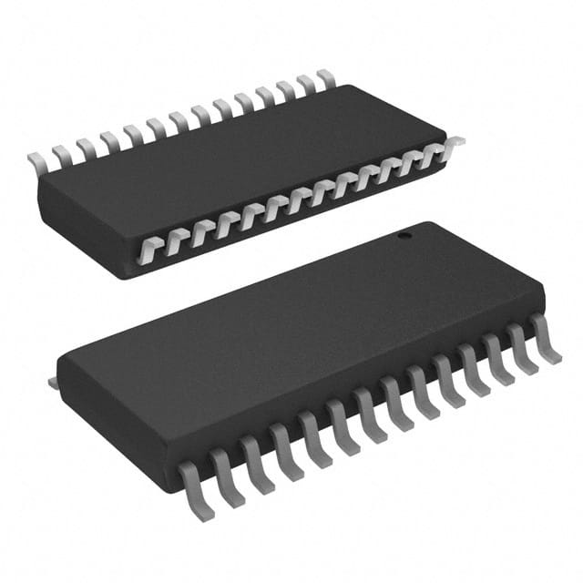
Texas Instruments UCC3750DW
- Part No.:
- UCC3750DW
- Manufacturer:
- Texas Instruments
- Category:
- Telecom
- Package:
- 28-SOIC (0.295", 7.50mm Width)
- Datasheet:
-
 UCC3750DW.pdf
- Description:
- IC TELECOM INTERFACE 28SOIC
- Quantity:
- Payment:

- Shipping:

Inventory:2,563
Please send an inquiry. Send us your inquiry, and we will respond immediately.
Product details
Overview
UCC3750DW from Texas Instruments is a dedicated source ringer controller IC for four-quadrant flyback-based telephone ring generators. It integrates a programmable sine-wave reference (20/25/50 Hz), 5V single-supply operation, charge-pump gate drive (12 V typical at VCP), and three high-current output drivers (GD1/GD2/GD3, 1.5 A pulsed) to control primary and synchronous secondary switches in isolated AC+DC ringing applications.
For engineers reviewing the UCC3750DW datasheet, UCC3750DW pinout, UCC3750DW application, or UCC3750DW equivalent, this device is selected for telecom line interface designs requiring precise low-frequency AC ringing with programmable amplitude, DC offset, and bi-directional power flow - especially where stable 48 V battery-referenced output and cycle-by-cycle DC current limiting are critical.
Technical Context
The UCC3750DW implements a mode-determined PWM architecture that separates error amplifier magnitude (MAG) and polarity (SIGN) to maintain loop stability across all four quadrants of ring signal generation. Its internal 32 kHz crystal-locked sine generator feeds a programmable divider (FS0/FS1) to produce low-THD (≤2%) 20/25/50 Hz outputs centered at 3 V with ±0.15 V offset tolerance.
It integrates a triangular oscillator (108–148 kHz, 3.0–4.75 V ramp), charge-pump circuit (VS1/VS2 switches, 10–30 Ω pull-up/down), and three independent gate drivers with matched rise/fall times (50–100 ns, CL = 2.7 nF). The DC current limit function activates when OUTDC exceeds 4.5 V or falls below 1.5 V, using externally set thresholds via R5/R6 ratio.
Key Specifications
| Parameter | Value and Actual Design Meaning |
|---|---|
| Sine Frequency Options | 20 Hz, 25 Hz, or 50 Hz - selectable via FS0/FS1 pins with 32 kHz crystal; enables compliance with global POTS ringing standards. |
| VCP Output Voltage | 11–14 V at 10 mA - powers high-side gate drivers without external boost, supporting MOSFETs up to 150 V drain-source rating. |
| Output Drive Current | 1.5 A pulsed - sufficient to directly drive gate transformers or low-Rds(on) discrete MOSFETs (Q1/Q2/Q3) in flyback topologies. |
| DC Current Limit Threshold | ±0.5 V (with R5/R6 = 3) - sets symmetrical overcurrent trip point referenced to VCM = 3 V, enabling fast cycle-by-cycle shutdown. |
| Internal Reference Voltage | 7.3–7.8 V (REF pin) - provides stable bias for error amplifiers and comparator circuits; requires ≥0.1 µF ceramic bypass to GND. |
| Operating Temperature Range | 0°C to +70°C - specified for commercial-grade telecom infrastructure applications with controlled ambient conditions. |
| Total Harmonic Distortion | ≤2% - ensures clean sinusoidal ringing waveform compliant with ITU-T K.21 surge immunity and audio quality requirements. |
Pinout & Package
UCC3750DW is housed in a 28-pin SOIC (DW) package with 0.300-inch body width, RoHS-compliant NiPdAu lead finish, and JEDEC Level-2 moisture sensitivity rating (260°C peak reflow).
| Pin/Terminal | Circuit Role | Design Meaning |
|---|---|---|
| GD1 | Primary switch driver | PWM-modulated output controlling Q1 during forward power transfer (Modes 1 & 3); requires gate-drive transformer isolation. |
| GD2 | p-Channel secondary driver | Inverted PWM output for Q2 (synchronous rectifier in Mode 1, reverse-power switch in Mode 4); logic-high disables conduction. |
| GD3 | n-Channel secondary driver | PWM output for Q3 (synchronous rectifier in Mode 3, reverse-power switch in Mode 2); non-inverted polarity for n-MOSFET gate drive. |
| SINREF | Internal sine reference output | High-impedance (≈25 kΩ), 0.5 VPK @ 3 V DC offset; requires 0.01–0.1 µF capacitor to GND for THD reduction. |
| OUTDC | DC current limit indicator | Active-high signal >4.5 V or <1.5 V triggers immediate PWM disable; used for fault latching or system-level protection coordination. |
| ENBL | Global enable input | TTL-compatible logic high (>2 V) enables all drivers and charge pump; pulled low disables outputs and reduces quiescent current to <100 µA. |
Key Features
| Feature | Design Value |
|---|---|
| Four-quadrant mode decoding | Automatically selects GD1/GD2/GD3 based on reference polarity and power flow direction - eliminates need for external state machine or microcontroller. |
| Programmable DC offset injection | Allows superposition of –48 V talk battery voltage onto AC ringing signal via NEG1/AMPIN path - enables single-ended line interface without floating supplies. |
| Charge-pump gate drive | Generates 12 V typical at VCP from 5 V VDD - supports efficient driving of high-voltage MOSFETs without auxiliary windings or external DC/DC converters. |
| Uncommitted amplifier (AMP) | Configurable as buffer, summing amp, or filter stage - used for DC offset scaling, SINFLT filtering, or custom signal conditioning before error amplifier input. |
| Zero-voltage relay switching aid | SWRLY output leads battery offset zero-crossings by ~5 ms - enables timing-critical mechanical relay control to minimize arcing and contact wear. |
Applications
| Central Office Line Card | VoIP Gateway Ringer |
|---|---|
Use Scenario: Generating standardized 20/25/50 Hz AC ringing signals on analog telephone lines powered from –48 V DC battery plant. IC Role / Device Role / Timing Role: Primary ring generator controller managing four-quadrant power flow, synchronous rectification, and DC offset injection to meet GR-909 and ITU-T K.20/K.21 requirements. Use Value: Eliminates need for discrete op-amps, oscillators, and protection logic - reduces BOM count by ≥7 components while maintaining <2% THD and ±1 Hz frequency accuracy. | Use Scenario: Adding PSTN-compatible ringing capability to IP-based residential gateways serving legacy analog phones. IC Role / Device Role / Timing Role: Isolated ring signal synthesizer interfacing between low-voltage digital control domain (MCU) and high-voltage analog line interface (transformer + MOSFETs). Use Value: Enables single 5 V supply operation with integrated charge pump - avoids dual-rail or isolated DC/DC for gate drive, simplifying power architecture and reducing layout area by ~35%. |
| Emergency Alert System Transmitter | Test Equipment Ring Simulator |
Use Scenario: Producing calibrated, high-reliability ringing waveforms for public safety alerting systems requiring fail-safe operation under wide temperature and load variations. IC Role / Device Role / Timing Role: Fault-tolerant ringer controller with cycle-by-cycle DC current limiting, RGOOD status flag, and SWRLY zero-crossing timing output for relay synchronization. Use Value: Provides hardware-enforced short-circuit protection and deterministic relay switching - meets UL 60950-1 Clause 4.6.2 and IEC 61000-4-5 surge immunity requirements without firmware intervention. | Use Scenario: Bench-level simulation of telephone line ringing behavior for protocol validation, codec testing, and hybrid coil characterization. IC Role / Device Role / Timing Role: Programmable waveform engine delivering adjustable amplitude, frequency, and DC offset - configurable via FS0/FS1, R5/R6, and external resistor networks. Use Value: Supports rapid reconfiguration between 20/25/50 Hz standards and arbitrary offset levels (0 to –48 V) - replaces multiple fixed-function test modules with one adaptable IC. |
Equivalent & Alternatives
The following parts are listed as comparable options for similar source ringer controller applications.
| Alternative Part | Technical Difference | Application Difference | Selection Advice |
|---|---|---|---|
| UCC2750DW | Wider operating temperature range (–40°C to +85°C); identical pinout and functional block diagram but different sine reference accuracy spec (±2 Hz vs. ±1 Hz). | Targeted at industrial or extended-temperature telecom equipment; not rated for commercial 0°C–70°C only applications. | Select UCC2750DW when ambient temperature may fall below 0°C or exceed 70°C; verify crystal stability over full range. |
| MAX14951 | Integrated H-bridge drivers (no external MOSFETs required); 3.3 V logic compatible; lacks programmable sine reference - relies on external DAC or MCU-generated waveform. | Designed for compact, low-component-count VoIP phone designs; does not support true four-quadrant flyback topology or battery-offset injection. | Choose MAX14951 for space-constrained consumer devices needing simplified layout; avoid if –48 V DC offset or crystal-based frequency accuracy is mandatory. |
Compared with UCC2750DW and MAX14951, the UCC3750DW uniquely combines crystal-referenced 20/25/50 Hz generation, –48 V DC offset support, and three independent gate drivers in a single SOIC-28 package - making it the only option for cost-sensitive, standards-compliant central office line cards requiring hardware-based four-quadrant control.
Availability
UCC3750DW is available at Aetrix Electronics and suitable for telecom infrastructure, VoIP gateway design, emergency alert transmitters, and test equipment requiring stable component supply with guaranteed long-term manufacturability and traceable sourcing.
Supply support for UCC3750DW includes scheduled delivery planning, volume procurement assistance, BOM continuity management, traceable sourcing, and lifecycle availability coordination for OEM customers, industrial embedded developers, connected-device designers, and electronics production programs.
Manufacturer
Texas Instruments is a global semiconductor leader specializing in analog, embedded processing, and connectivity technologies, with over 50 years of innovation in power management and signal chain solutions.
The UCC3750DW belongs to TI's Telecom Interface IC product line, engineered specifically for analog telephony applications including ringing, supervision, and line feeding - emphasizing precision timing, high-voltage isolation, and robust fault protection.
FAQ
What is the maximum allowable voltage on the VCP pin of the UCC3750DW?
The absolute maximum forced voltage on the VCP pin of the UCC3750DW is 13.2 V. Operation above this level risks permanent damage to the internal charge-pump circuitry. For reliable performance, maintain VCP between 11 V and 14 V under load (10 mA), using a ≥2.2 mF storage capacitor with low ESR to minimize ripple. Exceeding 13.2 V violates the Absolute Maximum Ratings table in the SLUS172C datasheet and voids TI's reliability guarantees for the UCC3750DW.
Can the UCC3750DW generate frequencies other than 20 Hz, 25 Hz, and 50 Hz?
Yes, the UCC3750DW can generate other frequencies by replacing the 32 kHz crystal with a different value or by applying an external clock signal to XTAL1 while grounding XTAL2. With a 32 kHz crystal, the internal divider yields exactly 20/25/50 Hz per FS0/FS1 settings. Substituting a 64 kHz crystal doubles those outputs; applying a 64 kHz square wave to XTAL1 produces the same result. The UCC3750DW datasheet confirms this flexibility in the "Sine Reference Generator" section, noting proportional scaling is preserved across all configurations.
How does the UCC3750DW implement four-quadrant operation without external logic?
The UCC3750DW implements four-quadrant operation through integrated mode-decoding circuitry that monitors the polarity of both the SINREF signal and the error amplifier output (SIGN/MAG). Based on these two inputs, it autonomously routes PWM signals to GD1, GD2, or GD3 - enabling forward/reverse power flow with positive/negative output voltage. This hardware-based decision logic, detailed in Table II and the "Control Logic and Outputs" section of the UCC3750DW datasheet, eliminates dependency on external microcontrollers or FPGA state machines.
What is the purpose of the SWRLY pin on the UCC3750DW?
The SWRLY pin on the UCC3750DW provides a logic-level timing signal that leads battery offset zero-crossings by approximately 5 ms, enabling zero-voltage switching of mechanical relays in telephone line interfaces. It sources up to 250 µA and is synchronized to the internal sine reference - allowing precise relay actuation just before voltage polarity reversal. This feature is explicitly documented in the "PIN DESCRIPTIONS" section of the UCC3750DW datasheet and is critical for minimizing contact arcing and extending relay service life.
Is the UCC3750DW pin-compatible with the UCC2750DW?
Yes, the UCC3750DW is pin-compatible with the UCC2750DW: both use identical SOIC-28 (DW) packages, share identical pin numbering and functions, and have fully overlapping electrical schematics. However, they differ in temperature rating (UCC3750DW: 0°C to +70°C; UCC2750DW: –40°C to +85°C) and sine reference accuracy (±1 Hz vs. ±2 Hz). The UCC3750DW datasheet confirms this compatibility in the "PACKAGE OPTION ADDENDUM" and "ELECTRICAL CHARACTERISTICS" tables.
UCC3750DW Specifications
- Product attributes
- Attribute value
- Manufacturer:
- Texas Instruments
- Series:
- -
- Package/Case:
- 28-SOIC (0.295", 7.50mm Width)
- Packaging:
- Bulk
- Product Status:
- Obsolete
- Function:
- Ring Generator Controller
- Interface:
- -
- Number of Circuits:
- 1
- Voltage - Supply:
- 5V
- Current - Supply:
- 500µA
- Power (Watts):
- -
- Operating Temperature:
- 0°C ~ 70°C
- Grade:
- -
- Qualification:
- -
- Mounting Type:
- Surface Mount
- Supplier Device Package:
- 28-SOIC
UCC3750DW FAQ
1.How can I place an order for UCC3750DW through Aetrix?
Please submit a Request for Quotation (RFQ) for UCC3750DW on Aetrix. Our sales agent will provide a competitive quotation and guide you through the order confirmation once you accept the terms.
2.Are the price and stock information for UCC3750DW reliable?
The price and inventory of UCC3750DW are updated periodically and may fluctuate due to market conditions. Stock and pricing data are typically refreshed every 24 hours. Quotation validity for UCC3750DW is usually 5 days.
3.What payment methods are accepted for UCC3750DW?
We accept Wire Transfer, PayPal, Credit Card, Western Union, MoneyGram, and Escrow for UCC3750DW transactions.
Note: Certain payment methods may incur a processing fee.
4.How is shipping managed for UCC3750DW?
UCC3750DW orders can be shipped via leading logistics carriers, including DHL, UPS, FedEx, TNT, or Registered Mail.
Once your UCC3750DW order is processed, you will receive an email with the shipment details and tracking number.
Note: Tracking information may take up to 24 hours to appear. Express delivery typically takes 3–5 business days.
5.How can I obtain technical support or documentation for UCC3750DW?
For technical support, including UCC3750DW datasheets, pinout diagrams, or application guidance, please contact our engineering support team. They can provide detailed documentation and assistance for your UCC3750DW requirements.
6.How does Aetrix verify that UCC3750DW is sourced from the original manufacturer or authorized distributors?
All UCC3750DW products on Aetrix are procured from qualified distributors and authorized channels. Our dedicated quality assurance team conducts strict verification, including traceability checks and, if necessary, third-party testing. This ensures that UCC3750DW meets industry standards.
7.What is the process for return or replacement of UCC3750DW?
All UCC3750DW units undergo pre-shipment inspection (PSI). If there is an issue with UCC3750DW, returns or replacements are accepted under the following conditions:
1.Quantity discrepancies, incorrect items, or visible external defects (such as breakage or corrosion), acknowledged by Aetrix.
2.The issue is reported within 90 days of delivery.
3.The UCC3750DW part is unused and in its original packaging.
Return procedure for UCC3750DW:
1.Submit a request within 90 days.
2.Obtain a Return Material Authorization (RMA) from Aetrix.
UCC3750DW Tags

-
LMC567CMX/NOPB
Texas Instruments
-
LM567CMX/NOPB
Texas Instruments
-
LM567CM/NOPB
Texas Instruments

-
VSC8531XMW-02
Microchip Technology
-
VSC8531XMW-05
Microchip Technology

-
GPY115C0VI
MaxLinear, Inc.

-
SI32185-A-FMR
Skyworks Solutions Inc.

-
VSC8541XMV-05
Microchip Technology

-
SI32178-B-FM1R
Skyworks Solutions Inc.
-
GPY215C0VI
MaxLinear, Inc.

-
CPC7514ZTR
Littelfuse Inc.

-
VSC8502XML-03
Microchip Technology
Tech Hub

A practical engineering guide to 3.3V and 5V logic compatibility, input thresholds, resistor dividers, translator ICs, MOSFET level shifting, I2C pull-ups, timing limits and power-sequencing risks.

The 74HC595 uses push-pull logic outputs, while the TPIC6B595 uses 50 V open-drain DMOS sinks for higher-power loads. This guide compares timing, current limits, 3.3 V interfacing, load wiring, thermal…

The 74HC595 converts serial data into eight stable parallel outputs. This guide covers pin functions, shift and storage timing, OE and MR behavior, drive-current limits, cascading, voltage compatibilit…

A technical comparison of level-sensitive latches and edge-triggered flip-flops, covering timing windows, setup and hold limits, master–slave operation, time borrowing, race-through, HDL inference and…

A D latch stores one bit while Enable controls when data can pass. This reference covers gate-level operation, truth tables, transparency, setup and hold timing, LE versus OE, common ICs and practical …

An SR latch stores one bit through cross-coupled feedback. This engineering reference covers NOR and NAND implementations, truth tables, forbidden-state recovery, gated operation, switch debouncing, fa…

Latch circuits retain one bit through feedback. This technical reference covers SR and D latches, truth tables, transparency, timing limits, latch-versus-flip-flop behavior, applications and common log…

An engineering guide to LED driver operation, constant-current and constant-voltage outputs, linear and switching topologies, dimming, IC selection, calculations, replacement compatibility, and fault c…

Operational amplifier guide covering op amp basics, feedback, ideal vs real op amps, common configurations, buffer circuits, offset, bias current, gain-bandwidth, slew rate, rail-to-rail limits and sel…

Jumper cables guide covering safe connection order, red and black clamp placement, final ground connection, cable gauge, length, clamp quality, copper vs CCA cables, jump starter comparison and battery…


