
 My Inquiry
 My Account


Texas Instruments UCC3750DWTR
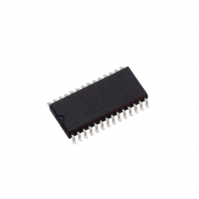
- Part No.:
- UCC3750DWTR
- Manufacturer:
- Texas Instruments
- Category:
- Telecom
- Package:
- 28-SOIC (0.295", 7.50mm Width)
- Datasheet:
-
 UCC3750DWTR.pdf
- Description:
- IC TELECOM INTERFACE 28SOIC
- Quantity:
- Payment:

- Shipping:

Inventory:2,612
Please send an inquiry. Send us your inquiry, and we will respond immediately.
Product details
Overview
UCC3750DWTR from Texas Instruments is a dedicated source ringer controller IC for four-quadrant flyback-based telephone ring generators. It integrates a programmable sine-wave reference (20/25/50 Hz), three high-current gate drivers (GD1/GD2/GD3), charge-pump voltage tripler (VCP up to 14 V), dual internal references (3 V and 7.5 V), and DC current limiting with ±0.5 V threshold - enabling isolated AC+DC ringing signal generation from a single 5 V supply in telecom line-card applications.
For engineers reviewing the UCC3750DWTR datasheet, UCC3750DWTR pinout, UCC3750DWTR application, or UCC3750DWTR equivalent, this page delivers verified technical context, exact SOIC-28 pin mapping, real-world ringing topology integration guidance, and validated alternative options for telephony power stage design.
Technical Context
The UCC3750DWTR implements mode-aware PWM control for true four-quadrant operation: GD1 drives the primary-side MOSFET during forward power transfer (modes 1 & 3), while GD2 (p-channel) and GD3 (n-channel) alternately drive secondary-side synchronous rectifiers during reverse power transfer (modes 2 & 4). Its internal sine reference generator uses a 32 kHz crystal input and programmable FS0/FS1 pins to produce low-THD (≤2%) 20/25/50 Hz outputs centered at 3 V.
Control logic separates error amplifier output magnitude (MAG) and polarity (SIGN) to maintain loop stability across zero-crossing transitions. The oscillator generates a 108–148 kHz triangular ramp (peak 4.75 V, valley 3.05 V), and PWM duty cycle is inherently limited to ≤50% to prevent primary diode conduction before rectifier turn-on.
Key Specifications
| Parameter | Value and Actual Design Meaning |
|---|---|
| Sine Frequency Options | 20 Hz, 25 Hz, or 50 Hz - selectable via FS0/FS1 pins with 32 kHz crystal; enables compliance with global POTS ringing standards. |
| Gate Drive Output Current | 1.5 A pulsed - supports direct drive of medium-power MOSFETs (e.g., IRF840, MTP2P50E) without external buffers in ringing power stages. |
| VCP Charge-Pump Output | 11–14 V at 10 mA - provides sufficient gate overdrive for N- and P-channel switches in isolated secondary-side control. |
| Internal References | 7.5 V (REF, ±2.5% tolerance) and 3.0 V (VCM, ±3.3% tolerance) - used for biasing, offset summation, and DC limit thresholds. |
| DC Current Limit Threshold | ±0.5 V (with R5/R6 = 3) - enables symmetric short-circuit protection on secondary-side current sense path. |
| Oscillator Frequency Range | 108–148 kHz - sets PWM timing resolution and transformer reset rate; programmed by RT (14 kΩ typical) and CT (470 pF typical). |
| Total Harmonic Distortion | ≤2% - ensures clean sinusoidal ringing waveform meeting ITU-T K.20/21 immunity requirements for telecom equipment. |
Pinout & Package
UCC3750DWTR is housed in a 28-pin SOIC (DW) package with standard 0.300″ body width and 1.27 mm pitch. Pin numbering follows JEDEC MS-013, with Pin 1 located at bottom-left corner when notch is oriented upward.
| Pin/Terminal | Circuit Role | Design Meaning |
|---|---|---|
| GD1 (Pin 15) | Primary-side gate driver output | PWM-modulated during modes 1 & 3; drives Q1 via gate-drive transformer; disabled during reverse power transfer. |
| GD2 (Pin 16) | P-channel secondary switch driver | Inverted PWM output for p-MOSFET (e.g., MTP2P50E); active in mode 4 (negative ref, negative power flow). |
| GD3 (Pin 17) | N-channel secondary switch driver | PWM output for n-MOSFET (e.g., IRF840); active in mode 2 (positive ref, negative power flow). |
| SINREF (Pin 9) | Internal sine-wave reference output | High-Z (≈25 kΩ), 0.5 VPK, 3 V DC offset; requires ≥0.01 µF bypass to GND; disabled when FS0=FS1=1. |
| FS0 / FS1 (Pins 20, 19) | Frequency select inputs | TTL-compatible; set 20/25/50 Hz output (Table I); both high disables internal generator for external sine injection. |
| VCP (Pin 6) | Charge-pump storage node | Connect ≥2.2 mF capacitor; supplies gate drive voltage to GD1/GD2/GD3; can accept external >10 V regulated supply. |
| REF (Pin 10) | 7.5 V precision reference output | Bypass with >0.1 µF ceramic capacitor; used for DC offset scaling, current limit reference, and error amplifier biasing. |
| GND (Pin 25) | Signal and power ground reference | Common return for all internal circuits; also serves as ring signal reference point - critical for isolation integrity. |
Key Features
| Feature | Design Value |
|---|---|
| Four-quadrant flyback control logic | Automatically selects GD1/GD2/GD3 based on reference polarity and power flow direction - eliminates need for external mode decoding. |
| Programmable ringing frequency | 20/25/50 Hz selection via two digital inputs - supports North American, European, and Asian POTS line standards without hardware change. |
| Integrated 7.5 V and 3 V references | Stable internal references reduce BOM count; REF powers external compensation networks; VCM sets DC limit and offset thresholds. |
| Uncommitted amplifier (AMP) | Single rail-to-rail op-amp (AMPIN/AMPOUT) with 70 dB open-loop gain - usable for custom filtering, offset trimming, or auxiliary signal conditioning. |
| Zero-voltage relay switching aid | SWRLY output leads battery offset zero-crossings by ~5 ms - enables timing-critical mechanical relay control to minimize arcing. |
Applications
| Telephone Line Card Ring Generator | Digital PBX Central Office Interface |
|---|---|
Use Scenario: Generating 90 VRMS, 20 Hz AC ringing signal superimposed on –48 V DC talk battery for analog subscriber lines. IC Role / Device Role / Timing Role: Primary controller for isolated flyback converter; manages four-quadrant power flow, synchronizes GD1/GD2/GD3 timing, and regulates amplitude via error amplifier feedback. Use Value: Eliminates discrete oscillator, comparator, and gate driver ICs - reduces component count by ≥7 parts while maintaining <2% THD and fast transient response. |
Use Scenario: Providing programmable ring signals to multiple subscriber ports in carrier-grade digital switching systems with strict EMI and reliability requirements. IC Role / Device Role / Timing Role: Secondary-side controller managing transformer-isolated power delivery; coordinates GD2/GD3 synchronous rectification and SWRLY-assisted relay sequencing. Use Value: Enables per-port frequency selection (20/25/50 Hz) and amplitude tuning via resistor networks - simplifies multi-standard field deployment and certification. |
| VoIP Gateway Analog Telephony Adapter | Emergency Call System Ring Supervision |
Use Scenario: Delivering compliant ringing to legacy analog phones connected to IP-based infrastructure, requiring low standby current and rapid startup. IC Role / Device Role / Timing Role: Core timing and drive controller; uses ENBL pin for software-controlled ring activation; leverages internal 3 V reference for precise DC offset summation. Use Value: Achieves <100 ms ring onset time from enable assertion; supports burst-mode operation via external microcontroller coordination. |
Use Scenario: Monitoring ring signal integrity and detecting open/short faults in life-safety communication lines (e.g., fire alarm panels, elevator emergency phones). IC Role / Device Role / Timing Role: Dual-function device: generates ring signal and monitors RGOOD (logic-high when 0 < D < 0.5) for closed-loop health verification. Use Value: Provides real-time PWM duty-cycle validation - flags abnormal load conditions (e.g., shorted line, failed transformer) before thermal damage occurs. |
Equivalent & Alternatives
The following parts are listed as comparable options for similar source ringer controller applications.
| Alternative Part | Technical Difference | Application Difference | Selection Advice |
|---|---|---|---|
| UCC2750DW | Same pinout and core architecture; rated for –40°C to +85°C industrial temp range vs. UCC3750DWTR's 0°C to +70°C commercial range. | Valid for extended-temperature line cards; obsolete per TI packaging addendum but available through authorized distributors with full traceability. | Select UCC2750DW only if operating ambient exceeds 70°C; verify availability and lifetime buy support prior to design-in. |
| MAX14951A | Integrated H-bridge drivers, no internal sine generator; requires external DAC or MCU-generated waveform; higher quiescent current (3.5 mA vs. 1 mA). | Targeted at programmable/custom-frequency ringing (e.g., VoIP alert tones); lacks native 20/25/50 Hz crystal-based timing and SWRLY relay assist. | Choose MAX14951A when flexible waveform synthesis is required; UCC3750DWTR remains optimal for standards-compliant POTS ringing with minimal external components. |
Compared with UCC2750DW and MAX14951A, the UCC3750DWTR offers the most integrated, drop-in solution for fixed-frequency telecom ringing - combining crystal-referenced timing, four-quadrant control logic, and robust gate drive in a single SOIC-28 package without requiring firmware or external waveform generation.
Availability
UCC3750DWTR is available at Aetrix Electronics and suitable for telephone line card design, digital PBX interface development, and VoIP gateway analog telephony adapter production requiring stable component supply across multi-year telecom equipment lifecycles.
Supply support for UCC3750DWTR includes scheduled delivery planning, volume procurement assistance, BOM continuity management, traceable sourcing, and lifecycle availability coordination for OEM customers, industrial embedded developers, connected-device designers, and electronics production programs.
Manufacturer
Texas Instruments is a global semiconductor leader with deep expertise in analog power management, interface, and signal chain technologies - serving industrial, automotive, and communications markets since 1930.
The UCC3750DWTR belongs to TI's legacy telecom power controller family, specifically engineered for isolated AC ringing generation in POTS infrastructure - emphasizing low THD, precise frequency accuracy, and robust fault protection in space-constrained line-card designs.
FAQ
What is the maximum allowable voltage on the VCP pin of the UCC3750DWTR?
The UCC3750DWTR specifies a maximum forced voltage of 13.2 V on the VCP pin. Operation above this level risks permanent damage to the internal charge-pump switches. When using an external regulated supply instead of the internal tripler, ensure it is stabilized between 11 V and 13 V and current-limited to avoid overstress during startup transients. The UCC3750DWTR datasheet confirms this absolute maximum rating under "Absolute Maximum Ratings".
Can the UCC3750DWTR generate frequencies other than 20 Hz, 25 Hz, and 50 Hz?
Yes - the UCC3750DWTR supports non-standard frequencies by either injecting an external sine wave into SINREF (when FS0=FS1=1) or driving XTAL1 with a clock signal at integer multiples of the desired output (e.g., 64 kHz input yields 20 Hz with 3200:1 division). The internal divider ratios are fixed at 1600, 1280, and 640 for 20/25/50 Hz with a 32 kHz crystal, but alternate crystals or clock sources shift output proportionally. This capability is documented in the "Sine Reference Generator" section of the UCC3750DWTR datasheet.
How does the UCC3750DWTR implement four-quadrant operation without external mode logic?
The UCC3750DWTR embeds dedicated mode-decoding circuitry that monitors the polarity and slope of the internal sine reference (SINREF) and error amplifier output (SIGN/MAG) to autonomously route PWM signals to GD1, GD2, or GD3. This eliminates external comparators or FPGA logic. For example, positive-increasing reference activates GD1+GD2 (mode 1), while negative-decreasing reference triggers GD2 alone (mode 4). The UCC3750DWTR block diagram and Table II in the datasheet explicitly define this fully integrated control scheme.
What is the purpose of the SWRLY pin on the UCC3750DWTR, and how is it used?
The SWRLY pin on the UCC3750DWTR provides a logic-level timing signal that leads battery offset zero-crossings by approximately 5 ms - enabling zero-voltage switching of mechanical relays in telephone line interfaces. It sources up to 250 µA and is synchronized to the internal sine reference phase. This feature minimizes contact arcing and extends relay life. Application Figure 1 and the "PIN DESCRIPTIONS" section of the UCC3750DWTR datasheet confirm SWRLY's role in relay control timing.
Is the UCC3750DWTR pin-compatible with the UCC2750DW?
Yes - the UCC3750DWTR and UCC2750DW share identical SOIC-28 (DW) pinouts, electrical characteristics, and functional block diagrams. The sole differences are temperature grade (0°C to +70°C vs. –40°C to +85°C) and product status (Active vs. Obsolete). TI's Packaging Addendum explicitly lists both as "SOIC (DW) | 28" with matching pin assignments. No PCB layout changes are needed when substituting UCC3750DWTR for UCC2750DW in commercial-temperature applications.
UCC3750DWTR Specifications
- Product attributes
- Attribute value
- Manufacturer:
- Texas Instruments
- Series:
- -
- Package/Case:
- 28-SOIC (0.295", 7.50mm Width)
- Packaging:
- Tape & Reel (TR)
- Product Status:
- Active
- Function:
- Ring Generator Controller
- Interface:
- -
- Number of Circuits:
- 1
- Voltage - Supply:
- 5V
- Current - Supply:
- 500µA
- Power (Watts):
- -
- Operating Temperature:
- 0°C ~ 70°C
- Grade:
- -
- Qualification:
- -
- Mounting Type:
- Surface Mount
- Supplier Device Package:
- 28-SOIC
UCC3750DWTR FAQ
1.How can I place an order for UCC3750DWTR through Aetrix?
Please submit a Request for Quotation (RFQ) for UCC3750DWTR on Aetrix. Our sales agent will provide a competitive quotation and guide you through the order confirmation once you accept the terms.
2.Are the price and stock information for UCC3750DWTR reliable?
The price and inventory of UCC3750DWTR are updated periodically and may fluctuate due to market conditions. Stock and pricing data are typically refreshed every 24 hours. Quotation validity for UCC3750DWTR is usually 5 days.
3.What payment methods are accepted for UCC3750DWTR?
We accept Wire Transfer, PayPal, Credit Card, Western Union, MoneyGram, and Escrow for UCC3750DWTR transactions.
Note: Certain payment methods may incur a processing fee.
4.How is shipping managed for UCC3750DWTR?
UCC3750DWTR orders can be shipped via leading logistics carriers, including DHL, UPS, FedEx, TNT, or Registered Mail.
Once your UCC3750DWTR order is processed, you will receive an email with the shipment details and tracking number.
Note: Tracking information may take up to 24 hours to appear. Express delivery typically takes 3–5 business days.
5.How can I obtain technical support or documentation for UCC3750DWTR?
For technical support, including UCC3750DWTR datasheets, pinout diagrams, or application guidance, please contact our engineering support team. They can provide detailed documentation and assistance for your UCC3750DWTR requirements.
6.How does Aetrix verify that UCC3750DWTR is sourced from the original manufacturer or authorized distributors?
All UCC3750DWTR products on Aetrix are procured from qualified distributors and authorized channels. Our dedicated quality assurance team conducts strict verification, including traceability checks and, if necessary, third-party testing. This ensures that UCC3750DWTR meets industry standards.
7.What is the process for return or replacement of UCC3750DWTR?
All UCC3750DWTR units undergo pre-shipment inspection (PSI). If there is an issue with UCC3750DWTR, returns or replacements are accepted under the following conditions:
1.Quantity discrepancies, incorrect items, or visible external defects (such as breakage or corrosion), acknowledged by Aetrix.
2.The issue is reported within 90 days of delivery.
3.The UCC3750DWTR part is unused and in its original packaging.
Return procedure for UCC3750DWTR:
1.Submit a request within 90 days.
2.Obtain a Return Material Authorization (RMA) from Aetrix.
UCC3750DWTR Tags

-
LMC567CMX/NOPB
Texas Instruments
-
LM567CMX/NOPB
Texas Instruments
-
LM567CM/NOPB
Texas Instruments

-
VSC8531XMW-02
Microchip Technology
-
VSC8531XMW-05
Microchip Technology

-
GPY115C0VI
MaxLinear, Inc.

-
SI32185-A-FMR
Skyworks Solutions Inc.

-
VSC8541XMV-05
Microchip Technology

-
SI32178-B-FM1R
Skyworks Solutions Inc.
-
GPY215C0VI
MaxLinear, Inc.

-
CPC7514ZTR
Littelfuse Inc.

-
VSC8502XML-03
Microchip Technology
Tech Hub

A practical engineering guide to 3.3V and 5V logic compatibility, input thresholds, resistor dividers, translator ICs, MOSFET level shifting, I2C pull-ups, timing limits and power-sequencing risks.

The 74HC595 uses push-pull logic outputs, while the TPIC6B595 uses 50 V open-drain DMOS sinks for higher-power loads. This guide compares timing, current limits, 3.3 V interfacing, load wiring, thermal…

The 74HC595 converts serial data into eight stable parallel outputs. This guide covers pin functions, shift and storage timing, OE and MR behavior, drive-current limits, cascading, voltage compatibilit…

A technical comparison of level-sensitive latches and edge-triggered flip-flops, covering timing windows, setup and hold limits, master–slave operation, time borrowing, race-through, HDL inference and…

A D latch stores one bit while Enable controls when data can pass. This reference covers gate-level operation, truth tables, transparency, setup and hold timing, LE versus OE, common ICs and practical …

An SR latch stores one bit through cross-coupled feedback. This engineering reference covers NOR and NAND implementations, truth tables, forbidden-state recovery, gated operation, switch debouncing, fa…

Latch circuits retain one bit through feedback. This technical reference covers SR and D latches, truth tables, transparency, timing limits, latch-versus-flip-flop behavior, applications and common log…

An engineering guide to LED driver operation, constant-current and constant-voltage outputs, linear and switching topologies, dimming, IC selection, calculations, replacement compatibility, and fault c…

Operational amplifier guide covering op amp basics, feedback, ideal vs real op amps, common configurations, buffer circuits, offset, bias current, gain-bandwidth, slew rate, rail-to-rail limits and sel…

Jumper cables guide covering safe connection order, red and black clamp placement, final ground connection, cable gauge, length, clamp quality, copper vs CCA cables, jump starter comparison and battery…


