
 My Inquiry
 My Account


Texas Instruments UCC3750DWTRG4
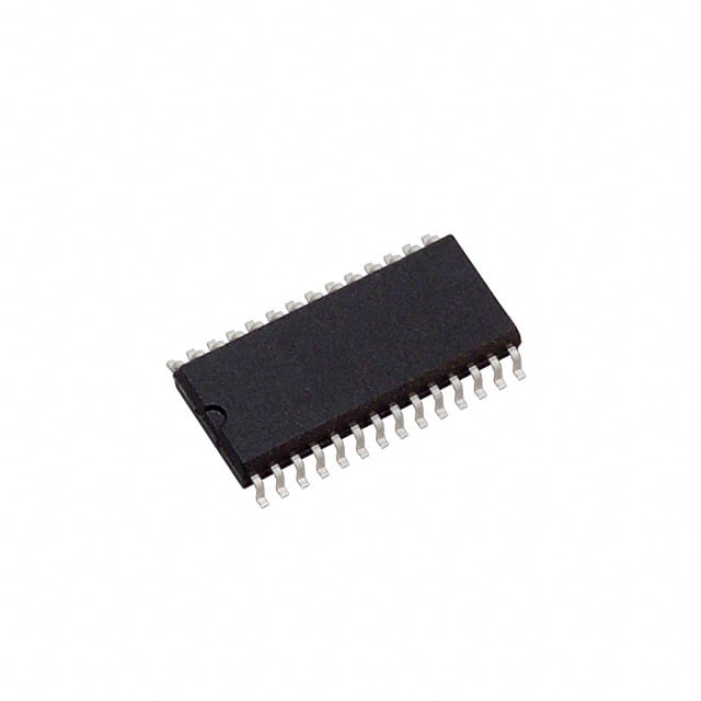
- Part No.:
- UCC3750DWTRG4
- Manufacturer:
- Texas Instruments
- Category:
- Telecom
- Package:
- 28-SOIC (0.295", 7.50mm Width)
- Datasheet:
-
 UCC3750DWTRG4.pdf
- Description:
- IC TELECOM INTERFACE 28SOIC
- Quantity:
- Payment:

- Shipping:

Inventory:1,973
Please send an inquiry. Send us your inquiry, and we will respond immediately.
Product details
Overview
UCC3750DWTRG4 from Texas Instruments is a dedicated source ringer controller IC for four-quadrant flyback-based telephone ring generators, providing full control of primary and dual secondary synchronous rectifier switches (GD1, GD2, GD3), onboard 20/25/50Hz sine-wave reference (±1Hz accuracy), programmable DC current limiting (±0.5V threshold), and charge-pump gate drive voltage generation (11–14V at 10mA). It operates from a single 5V supply and targets telecom line card applications requiring isolated AC+DC ringing signals.
For engineers reviewing the UCC3750DWTRG4 datasheet, UCC3750DWTRG4 pinout, UCC3750DWTRG4 application, or UCC3750DWTRG4 equivalent, key selection considerations include its 28-pin SOIC-DW package, four-quadrant power flow management, internal 7.5V reference with ±60mV load regulation, 50% maximum PWM duty cycle for inherent current limiting, and compatibility with 32kHz crystal or external sine-wave injection at SINREF.
Technical Context
The UCC3750DWTRG4 implements a mode-decoding architecture that separates error amplifier output magnitude (MAG) and polarity (SIGN) to dynamically assign PWM drive to GD1 (primary switch), GD2 (p-channel secondary), or GD3 (n-channel secondary) based on real-time reference polarity and power flow direction-enabling true bidirectional voltage and power transfer across all four quadrants. Its internal oscillator generates a 108–148kHz triangular ramp (peak 4.75V, valley 3.05V) synchronized to CT/RT timing components.
It integrates a high-impedance (≈25kΩ) sine-reference generator with <2% THD, buffered SINFLT output, and dual-frequency-select pins (FS0/FS1) that configure 20Hz, 25Hz, or 50Hz outputs when driven by a 32kHz crystal; disabling the internal generator (FS0=FS1=1) allows external sine-wave injection at SINREF with matching 3V DC offset. The uncommitted amplifier (AMPIN/AMPOUT) supports custom signal conditioning for offset summation or feedback compensation.
Key Specifications
| Parameter | Value and Actual Design Meaning |
|---|---|
| Sine Reference Frequency | 20Hz, 25Hz, or 50Hz (programmable via FS0/FS1; ±1Hz accuracy at TJ = 25°C) |
| Internal Reference Voltage | 7.5V (REF pin; ±60mV load regulation over 0–2mA, enabling stable biasing of external circuitry) |
| Gate Drive Output Current | 1.5A pulsed (GD1/GD2/GD3; sufficient to directly drive MOSFET gates without external buffers in telecom ring circuits) |
| Charge Pump Output Voltage | 11–14V at 10mA (VCP pin; powers high-side gate drivers, eliminating need for external high-voltage supplies) |
| DC Current Limit Threshold | ±0.5V (NEGDC input; symmetric trip point enables short-circuit protection during both positive and negative power flow modes) |
| Maximum PWM Duty Cycle | 50% (inherent limit from oscillator ramp shape; prevents primary rectifier conduction overlap and ensures safe transformer reset) |
| Operating Temperature Range | 0°C to +70°C (commercial grade; validated for line card environments with controlled thermal management) |
Pinout & Package
UCC3750DWTRG4 is housed in a 28-pin SOIC (DW) package with standard 0.300-inch body width and gull-wing leads. Pin numbering follows JEDEC MS-013, with Pin 1 located at the top-left corner adjacent to the index mark.
| Pin/Terminal | Circuit Role | Design Meaning |
|---|---|---|
| GD1 (Pin 25) | Primary-side PWM driver output | Drives gate of primary switch Q1 during forward power transfer (Modes 1 & 3); zero output during reverse transfer |
| GD2 (Pin 27) | p-Channel secondary rectifier driver | Inverted PWM output for p-MOSFET Q2; active in Mode 1 (forward +ve) and Mode 4 (reverse –ve) |
| GD3 (Pin 26) | n-Channel secondary rectifier driver | PWM output for n-MOSFET Q3; active in Mode 2 (reverse +ve) and Mode 3 (forward –ve) |
| SINREF (Pin 9) | Internal sine-wave reference output | High-impedance (≈25kΩ) 20/25/50Hz sine output centered at 3V; requires ≥0.01µF bypass to GND |
| FS0 / FS1 (Pins 20, 19) | Frequency select inputs | TTL-compatible logic inputs selecting sine frequency: 00=20Hz, 10=25Hz, 01=50Hz, 11=disabled |
| VCP (Pin 6) | Charge pump storage node | Connects to ≥2.2mF capacitor; supplies 11–14V gate drive voltage to GD1/GD2/GD3 drivers |
| REF (Pin 10) | 7.5V precision reference output | Internally regulated; bypass with >0.1µF ceramic capacitor to ensure stability of external circuitry |
| ENBL (Pin 23) | Global enable input | Active-high logic input enabling all outputs and charge pump; pull low to fully disable device |
Key Features
| Feature | Design Value |
|---|---|
| Four-quadrant flyback control logic | Automatically routes PWM to GD1/GD2/GD3 based on real-time SIGN/MAG signals and reference polarity-enabling bidirectional voltage and power flow without external mode switching |
| Programmable ringing frequency | 20Hz, 25Hz, or 50Hz selectable via two logic pins; supports global PSTN standards (North America, UK, EU) with no component changes |
| Integrated charge pump | Generates 11–14V gate drive from 5V VDD supply; eliminates need for external high-voltage bias rails in isolated secondary-side implementations |
| DC current limit with symmetric thresholds | ±0.5V trip points at NEGDC (with R5/R6 = 3); provides cycle-by-cycle short-circuit protection during both forward and reverse power transfer |
| Uncommitted operational amplifier | AMPIN/AMPOUT pins support configurable DC offset summation, feedback compensation, or auxiliary signal processing-reducing external component count |
Applications
| Telephone Line Card Ring Generator | Digital PBX Central Office Interface |
|---|---|
Use Scenario: Generating 90VRMS AC ringing signal superimposed on –48V DC battery feed for analog telephone lines in carrier-grade line cards. IC Role / Device Role / Timing Role: Primary controller managing four-quadrant flyback topology, synchronizing GD1/GD2/GD3 outputs to reference waveform polarity and power flow direction. Use Value: Enables single-chip implementation of compliant 20Hz/25Hz/50Hz ringing with <2% THD and programmable amplitude/offset-replacing discrete op-amp and logic solutions. |
Use Scenario: Providing isolated, regulated ringing voltage to multiple subscriber lines in digital PBX systems requiring simultaneous multi-line alerting. IC Role / Device Role / Timing Role: Source ringer controller coordinating synchronous rectification and bidirectional energy recovery across transformer windings to maintain efficiency during ring burst intervals. Use Value: Reduces thermal stress and improves power efficiency by recovering energy during reverse power transfer (Modes 2 & 4), extending line card uptime and reducing cooling requirements. |
| VoIP Gateway Analog Telephony Adapter (ATA) | Emergency Alert System (EAS) Ring Tone Generator |
Use Scenario: Converting VoIP session signaling into legacy POTS-compatible ringing signals for analog phones connected to residential gateways. IC Role / Device Role / Timing Role: Sine-reference generator and PWM modulator producing precise 20Hz ringing (US standard) with adjustable DC offset to match local loop impedance. Use Value: Eliminates need for external crystal oscillators and discrete driver stages-reducing BOM cost and PCB area while ensuring FCC Part 68 compliance. |
Use Scenario: Generating standardized emergency alert tones (e.g., EIA RS-189A) requiring accurate low-frequency AC waveforms with tight amplitude stability. IC Role / Device Role / Timing Role: Precision sine-wave reference source and amplitude-controlled output driver delivering repeatable 20Hz/25Hz signals with <2% THD under varying load conditions. Use Value: Guarantees regulatory compliance through factory-trimmed reference accuracy (±1Hz) and low-distortion output-critical for public safety infrastructure reliability. |
Equivalent & Alternatives
The following parts are listed as comparable options for similar source ringer controller applications.
| Alternative Part | Technical Difference | Application Difference | Selection Advice |
|---|---|---|---|
| UCC2750DW | Same pinout and core functionality but rated for –40°C to +85°C industrial temperature range; obsolete status limits long-term availability | Preferred for extended-temperature line cards where ambient exceeds 70°C; not suitable for new designs due to obsolescence | Select only if legacy replacement is required and industrial temp range is mandatory; verify RoHS and MSL compliance for existing stock |
| MAX14951ATL+ | Integrated H-bridge driver with embedded microcontroller; supports programmable frequency (1–100Hz), higher peak output (±120V), but requires external MCU firmware | Targets smart ring generators with dynamic tone sequencing and diagnostics; lacks native four-quadrant flyback control logic | Choose when advanced features like tone modulation or fault logging are needed; avoid if seeking drop-in replacement for UCC3750DWTRG4's analog control architecture |
Compared with UCC2750DW and MAX14951ATL+, the UCC3750DWTRG4 delivers optimized analog four-quadrant control with minimal external components, commercial-grade thermal performance, and guaranteed sine-reference accuracy-making it ideal for cost-sensitive, high-volume telecom line card designs where simplicity and proven reliability are prioritized.
Availability
UCC3750DWTRG4 is available at Aetrix Electronics and suitable for telephone line card design, digital PBX interface development, and VoIP gateway analog telephony adapter (ATA) production requiring stable component supply, consistent parametric performance, and long-term manufacturability assurance.
Supply support for UCC3750DWTRG4 includes scheduled delivery planning, volume procurement assistance, BOM continuity management, traceable sourcing, and lifecycle availability coordination for OEM customers, industrial embedded developers, connected-device designers, and electronics production programs.
Manufacturer
Texas Instruments is a global semiconductor leader specializing in analog, embedded processing, and connectivity technologies, with decades of experience in power management and interface ICs for communications infrastructure.
The UCC3750DWTRG4 belongs to TI's telecom power controller product line, designed specifically for isolated ringing signal generation in analog telephony systems-emphasizing precision sine-wave synthesis, four-quadrant energy recovery, and robust operation in noisy line-card environments.
FAQ
What is the operating temperature range for the UCC3750DWTRG4?
The UCC3750DWTRG4 is specified for operation from 0°C to +70°C, aligning with commercial-grade requirements for telecom line cards housed in temperature-controlled central office or enterprise environments. This range is validated per the electrical characteristics table in the SLUS172C datasheet, where all parameters-including sine reference accuracy and gate drive current-are guaranteed across this span. The UCC3750DWTRG4 does not support extended industrial temperatures; for –40°C to +85°C operation, the obsolete UCC2750DW was historically used.
How does the UCC3750DWTRG4 achieve four-quadrant operation?
The UCC3750DWTRG4 achieves four-quadrant operation through integrated mode-decoding logic that monitors the polarity and slope of the internal sine reference (SINREF) and the error amplifier output (SIGN/MAG). Based on these signals, it dynamically assigns PWM drive to GD1 (primary switch), GD2 (p-channel secondary), or GD3 (n-channel secondary) to manage forward/reverse power flow and positive/negative output voltage-enabling true bidirectional energy transfer without external logic. This is implemented in hardware, not firmware.
Can the UCC3750DWTRG4 accept an external sine-wave input?
Yes-the UCC3750DWTRG4 can accept an external sine-wave input at the SINREF pin when both FS0 and FS1 are set high (logic 1). In this configuration, the internal sine-wave generator is disabled, and the external signal must be centered at 3V DC offset to match the internal reference level. This allows custom frequencies beyond 20/25/50Hz or integration with system-level clock sources, provided the external signal meets the input voltage limits (–0.3V to 7.5V).
What is the purpose of the RGOOD pin on the UCC3750DWTRG4?
The RGOOD pin on the UCC3750DWTRG4 is a logic-level indicator that signals when the error amplifier output (OUT2) is within its valid operating range (0 < duty cycle < 0.5). It sources up to 0.5mA and is typically used to enable downstream monitoring circuits or provide feedback to system controllers. When RGOOD is high, it confirms stable closed-loop regulation; if low, it indicates saturation or instability-helping diagnose issues like incorrect compensation or excessive load transients in the ring generator circuit.
Does the UCC3750DWTRG4 require external components for the charge pump function?
Yes-the UCC3750DWTRG4 requires external components for the charge pump: VS1 and VS2 connect to external flying capacitors (typically 1–2.2µF), and VCP connects to a storage capacitor ≥2.2mF (e.g., aluminum or tantalum) to minimize ripple. These components form a voltage tripler circuit that boosts the 5V VDD supply to 11–14V for gate drive. Leaving VS1/VS2 disconnected while applying a regulated >10V supply directly to VCP is also supported, offering flexibility in layout-constrained designs.
UCC3750DWTRG4 Specifications
- Product attributes
- Attribute value
- Manufacturer:
- Texas Instruments
- Series:
- -
- Package/Case:
- 28-SOIC (0.295", 7.50mm Width)
- Packaging:
- Tape & Reel (TR)
- Product Status:
- Discontinued at Digi-Key
- Function:
- Ring Generator Controller
- Interface:
- -
- Number of Circuits:
- 1
- Voltage - Supply:
- 5V
- Current - Supply:
- 500µA
- Power (Watts):
- -
- Operating Temperature:
- 0°C ~ 70°C
- Grade:
- -
- Qualification:
- -
- Mounting Type:
- Surface Mount
- Supplier Device Package:
- 28-SOIC
UCC3750DWTRG4 FAQ
1.How can I place an order for UCC3750DWTRG4 through Aetrix?
Please submit a Request for Quotation (RFQ) for UCC3750DWTRG4 on Aetrix. Our sales agent will provide a competitive quotation and guide you through the order confirmation once you accept the terms.
2.Are the price and stock information for UCC3750DWTRG4 reliable?
The price and inventory of UCC3750DWTRG4 are updated periodically and may fluctuate due to market conditions. Stock and pricing data are typically refreshed every 24 hours. Quotation validity for UCC3750DWTRG4 is usually 5 days.
3.What payment methods are accepted for UCC3750DWTRG4?
We accept Wire Transfer, PayPal, Credit Card, Western Union, MoneyGram, and Escrow for UCC3750DWTRG4 transactions.
Note: Certain payment methods may incur a processing fee.
4.How is shipping managed for UCC3750DWTRG4?
UCC3750DWTRG4 orders can be shipped via leading logistics carriers, including DHL, UPS, FedEx, TNT, or Registered Mail.
Once your UCC3750DWTRG4 order is processed, you will receive an email with the shipment details and tracking number.
Note: Tracking information may take up to 24 hours to appear. Express delivery typically takes 3–5 business days.
5.How can I obtain technical support or documentation for UCC3750DWTRG4?
For technical support, including UCC3750DWTRG4 datasheets, pinout diagrams, or application guidance, please contact our engineering support team. They can provide detailed documentation and assistance for your UCC3750DWTRG4 requirements.
6.How does Aetrix verify that UCC3750DWTRG4 is sourced from the original manufacturer or authorized distributors?
All UCC3750DWTRG4 products on Aetrix are procured from qualified distributors and authorized channels. Our dedicated quality assurance team conducts strict verification, including traceability checks and, if necessary, third-party testing. This ensures that UCC3750DWTRG4 meets industry standards.
7.What is the process for return or replacement of UCC3750DWTRG4?
All UCC3750DWTRG4 units undergo pre-shipment inspection (PSI). If there is an issue with UCC3750DWTRG4, returns or replacements are accepted under the following conditions:
1.Quantity discrepancies, incorrect items, or visible external defects (such as breakage or corrosion), acknowledged by Aetrix.
2.The issue is reported within 90 days of delivery.
3.The UCC3750DWTRG4 part is unused and in its original packaging.
Return procedure for UCC3750DWTRG4:
1.Submit a request within 90 days.
2.Obtain a Return Material Authorization (RMA) from Aetrix.
UCC3750DWTRG4 Tags

-
LMC567CMX/NOPB
Texas Instruments
-
LM567CMX/NOPB
Texas Instruments
-
LM567CM/NOPB
Texas Instruments

-
VSC8531XMW-02
Microchip Technology
-
VSC8531XMW-05
Microchip Technology

-
GPY115C0VI
MaxLinear, Inc.

-
SI32185-A-FMR
Skyworks Solutions Inc.

-
VSC8541XMV-05
Microchip Technology

-
SI32178-B-FM1R
Skyworks Solutions Inc.
-
GPY215C0VI
MaxLinear, Inc.

-
CPC7514ZTR
Littelfuse Inc.

-
VSC8502XML-03
Microchip Technology
Tech Hub

A practical engineering guide to 3.3V and 5V logic compatibility, input thresholds, resistor dividers, translator ICs, MOSFET level shifting, I2C pull-ups, timing limits and power-sequencing risks.

The 74HC595 uses push-pull logic outputs, while the TPIC6B595 uses 50 V open-drain DMOS sinks for higher-power loads. This guide compares timing, current limits, 3.3 V interfacing, load wiring, thermal…

The 74HC595 converts serial data into eight stable parallel outputs. This guide covers pin functions, shift and storage timing, OE and MR behavior, drive-current limits, cascading, voltage compatibilit…

A technical comparison of level-sensitive latches and edge-triggered flip-flops, covering timing windows, setup and hold limits, master–slave operation, time borrowing, race-through, HDL inference and…

A D latch stores one bit while Enable controls when data can pass. This reference covers gate-level operation, truth tables, transparency, setup and hold timing, LE versus OE, common ICs and practical …

An SR latch stores one bit through cross-coupled feedback. This engineering reference covers NOR and NAND implementations, truth tables, forbidden-state recovery, gated operation, switch debouncing, fa…

Latch circuits retain one bit through feedback. This technical reference covers SR and D latches, truth tables, transparency, timing limits, latch-versus-flip-flop behavior, applications and common log…

An engineering guide to LED driver operation, constant-current and constant-voltage outputs, linear and switching topologies, dimming, IC selection, calculations, replacement compatibility, and fault c…

Operational amplifier guide covering op amp basics, feedback, ideal vs real op amps, common configurations, buffer circuits, offset, bias current, gain-bandwidth, slew rate, rail-to-rail limits and sel…

Jumper cables guide covering safe connection order, red and black clamp placement, final ground connection, cable gauge, length, clamp quality, copper vs CCA cables, jump starter comparison and battery…


