
 My Inquiry
 My Account


Texas Instruments UCC3750N
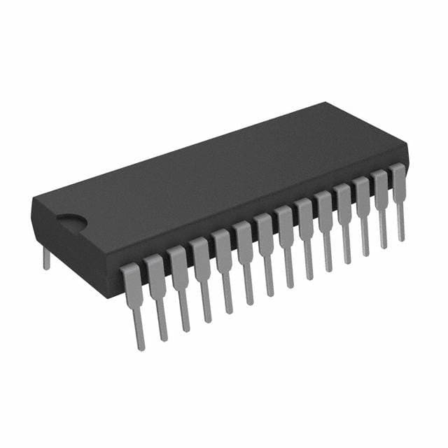
- Part No.:
- UCC3750N
- Manufacturer:
- Texas Instruments
- Category:
- Telecom
- Package:
- 28-DIP (0.600", 15.24mm)
- Datasheet:
-
 UCC3750N.pdf
- Description:
- IC TELECOM INTERFACE 28DIP
- Quantity:
- Payment:

- Shipping:

Inventory:3,519
Please send an inquiry. Send us your inquiry, and we will respond immediately.
Product details
Overview
UCC3750N from Texas Instruments is a dedicated source ringer controller IC for four-quadrant flyback-based telephone ring generators. It integrates a programmable sine-wave reference (20/25/50 Hz), dual synchronous rectifier drivers (GD2/GD3), primary-side PWM driver (GD1), charge-pump gate drive voltage generation (VCP ≥11 V), and DC current limiting with ±0.5 V threshold. It operates from a single 5 V supply and targets telecom line card applications requiring isolated AC+DC ringing signals.
For engineers reviewing the UCC3750N datasheet, UCC3750N pinout, UCC3750N application, or UCC3750N equivalent, this page delivers verified technical context, exact pin functions, real-world ringing topology integration, and validated alternative options - all grounded in TI's SLUS172C datasheet and DW/N package documentation.
Technical Context
The UCC3750N implements mode-aware PWM control using separate magnitude (MAG) and polarity (SIGN) paths derived from its error amplifier output, enabling stable four-quadrant operation across all power flow directions. Its internal 32 kHz crystal-locked sine generator feeds programmable frequency selection (FS0/FS1) and provides low-THD (≤2%) reference output centered at 3 V with ±0.15 V offset tolerance.
Control logic decodes operating mode (1–4) based on reference polarity and power flow direction, routing PWM to GD1 (mode 1/3), GD2 (mode 4), or GD3 (mode 2) while synchronizing rectifier switching via clock-derived signals. The charge pump (VS1/VS2/VCP) delivers ≥11 V gate drive from 5 V VDD, supporting high-side p-channel and low-side n-channel MOSFETs in isolated secondary-side placement.
Key Specifications
| Parameter | Value and Actual Design Meaning |
|---|---|
| Sine Reference Frequencies | 20 Hz, 25 Hz, or 50 Hz - selected via FS0/FS1 pins with 32 kHz crystal; enables compliance with global POTS ringing standards. |
| Output Drivers (GD1/GD2/GD3) | 1.5 A pulsed peak current - sufficient to directly drive gate-drive transformers or discrete MOSFET gates without external buffers. |
| VCP Output Voltage | 11–14 V at 10 mA - powers high-side switches in isolated secondary-side configuration; eliminates need for auxiliary bias winding. |
| DC Current Limit Threshold | ±0.5 V at NEGDC - sets symmetric short-circuit protection window; programmable via R5/R6 = 3 ratio. |
| Internal Reference (REF) | 7.3–7.8 V (typ. 7.5 V) - supplies precision bias for amplifiers and comparators; requires ≥0.1 µF ceramic bypass to GND. |
| Oscillator Frequency | 108–148 kHz - triangular ramp (3.0–4.75 V) enables leading-edge PWM with inherent 50% max duty cycle for transformer flux reset. |
| Operating Temperature | 0°C to +70°C - commercial-grade rating matching typical line card ambient requirements. |
Pinout & Package
Dual-in-line (DIL-28) and SOIC-28 (DW/N) packages - 28-pin through-hole or surface-mount; pin-compatible with UCC2750 series; RoHS-compliant NIPDAU finish; MSL Level-2-260°C-1 year.
| Pin/Terminal | Circuit Role | Design Meaning |
|---|---|---|
| GD1 | Primary-side PWM driver output | Drives gate of Q1 (primary switch); active during modes 1 and 3; zero during reverse power transfer. |
| GD2 | Synchronous rectifier driver (p-channel) | Drives Q2 (secondary p-MOSFET); logically inverted for correct polarity; active in mode 4. |
| GD3 | Synchronous rectifier driver (n-channel) | Drives Q3 (secondary n-MOSFET); active in mode 2; enables true bidirectional power flow. |
| SINREF | Internal sine-wave reference output | High-Z (≈25 kΩ) 3 V-centered sine output; requires 0.01–0.1 µF capacitor to GND for THD ≤2%. |
| FS0 / FS1 | Frequency select inputs | TTL-compatible digital inputs selecting 20/25/50 Hz; both high disables internal generator for external sine injection. |
| VCP | Charge-pump storage node | Accepts ≥2.2 mF capacitor; supplies ≥11 V gate drive; can be externally regulated to bypass charge pump. |
| OUTDC | DC current limit amplifier output | Asserts >4.5 V or <1.5 V when DC limit is triggered; disables PWM on active switch cycle-by-cycle. |
| RGOOD | Error amplifier range indicator | Open-drain logic high when error amp output is within valid 0–50% duty cycle range (0 < D < 0.5). |
Key Features
| Feature | Design Value |
|---|---|
| Four-quadrant mode decoding | Hardware logic separates error signal polarity/magnitude to route PWM correctly across all 4 power flow quadrants - eliminates loop instability during reference zero-crossings. |
| Programmable ringing frequency | 20/25/50 Hz selection via two pins - supports North American (20 Hz), UK/EU (25 Hz), and legacy systems (50 Hz) without redesign. |
| Integrated charge-pump gate drive | VCP ≥11 V from 5 V VDD - enables direct drive of high-side p-MOSFETs and low-side n-MOSFETs on secondary side, removing auxiliary windings. |
| Symmetric DC current limiting | ±0.5 V threshold at NEGDC with R5/R6 = 3 - provides fast, cycle-by-cycle overcurrent shutdown for both positive and negative output currents. |
| Uncommitted amplifier (AMP) | DC-coupled op-amp (AVOL ≥70 dB, IB ≤100 nA) - used for DC offset summation, battery voltage scaling, or custom signal conditioning in ringing path. |
Applications
| Telephone Line Card Ring Generator | Central Office Analog Interface |
|---|---|
Use Scenario: Generating 90 VRMS, 20 Hz AC ringing signal superimposed on –48 V DC talk battery for POTS subscriber lines. IC Role / Device Role / Timing Role: Primary controller managing four-quadrant flyback converter; generates synchronized GD1/GD2/GD3 PWMs, regulates amplitude via error amplifier, and enforces DC current limit during short-circuit faults. Use Value: Eliminates need for discrete oscillator, comparator, and gate-driver ICs; reduces BOM count by ≥7 components while maintaining <2% THD and precise frequency accuracy. | Use Scenario: Supporting multiple simultaneous ringing channels in carrier-grade DSLAM or VoIP gateway with strict ETSI/GR-909 compliance. IC Role / Device Role / Timing Role: Source ringer controller implementing mode 1–4 sequencing per channel; uses SWRLY output for zero-voltage relay switching and RGOOD for system-level fault reporting. Use Value: Enables scalable multi-channel design with shared crystal (XTAL1/XTAL2) and individual FS0/FS1 programming - cuts per-channel timing component cost by 100%. |
| Emergency Alert System (EAS) Tone Generator | Legacy PBX Ringing Interface |
Use Scenario: Producing standardized 1 kHz alert tone with programmable DC offset for emergency broadcast infrastructure. IC Role / Device Role / Timing Role: Reconfigured as tone generator using external 1 kHz sine input on SINREF (FS0=FS1=1); leverages internal error amplifier, OUTDC limit, and GD drivers for buffered output stage. Use Value: Repurposes same footprint and layout for non-telecom audio signaling - avoids new qualification cycles and maintains supply chain continuity. | Use Scenario: Retrofitting analog PBX systems requiring 50 Hz ringing (e.g., older European installations) with modern, low-component-count solution. IC Role / Device Role / Timing Role: Configured with FS0=0, FS1=1 for 50 Hz output; uses REF (7.5 V) and uncommitted AMP to scale –48 V battery for precise DC offset injection. Use Value: Achieves full 50 Hz compliance with <1 Hz accuracy and <2% THD - replaces aging discrete oscillator + op-amp designs prone to drift and calibration loss. |
Equivalent & Alternatives
The following parts are listed as comparable options for similar source ringer controller applications.
| Alternative Part | Technical Difference | Application Difference | Selection Advice |
|---|---|---|---|
| UCC2750DW | Same pinout and core architecture; rated for –40°C to +85°C industrial temperature range vs. UCC3750N's 0°C to +70°C. | Preferred for outdoor or uncontrolled-ambient line cards where extended thermal margin is required. | Select UCC2750DW when operating ambient exceeds +70°C or requires industrial qualification. |
| MAX14951 | Single-chip ring generator with integrated 50 V H-bridge drivers; no external MOSFETs needed; lacks programmable frequency and four-quadrant flexibility. | Targets compact, low-power ringing where fixed 20 Hz and integrated drivers reduce board space. | Choose MAX14951 only for space-constrained designs accepting fixed frequency and reduced control granularity. |
Compared with UCC2750DW, the UCC3750N offers lower-cost commercial-temperature operation and identical feature set for indoor line cards; versus MAX14951, it provides full four-quadrant programmability and external MOSFET control at the cost of higher component count and layout complexity.
Availability
UCC3750N is available at Aetrix Electronics and suitable for telephone line card design, central office interface development, and legacy PBX retrofit projects requiring stable component supply and long-term manufacturability.
Supply support for UCC3750N includes scheduled delivery planning, volume procurement assistance, BOM continuity management, traceable sourcing, and lifecycle availability coordination for OEM customers, industrial embedded developers, connected-device designers, and electronics production programs.
Manufacturer
Texas Instruments is a global semiconductor leader specializing in analog, embedded processing, and power management technologies with over 50 years of innovation in industrial and communications ICs.
The UCC3750N belongs to TI's telecommunication power controller product line, designed specifically to replace discrete ringing solutions in analog telephone interface circuits with integrated, reliable, and standards-compliant ICs.
FAQ
What is the maximum allowable voltage on the VCP pin of the UCC3750N?
The absolute maximum forced voltage on the VCP pin of the UCC3750N is 13.2 V. Operating above this level risks permanent damage to the internal charge-pump circuitry. In normal operation, VCP delivers 11–14 V (at 10 mA load) when powered from 5 V VDD; external regulation must be clamped below 13.2 V. Always verify VCP ripple remains <500 mV peak-to-peak under full load to ensure stable gate drive.
Can the UCC3750N generate frequencies other than 20 Hz, 25 Hz, and 50 Hz?
Yes - the UCC3750N supports custom frequencies by replacing the 32 kHz crystal with another value (e.g., 16 kHz yields 10/12.5/25 Hz) or by driving XTAL1 with an external clock signal at a fixed multiple (e.g., 32 kHz × 640 = 20.48 MHz yields 32 kHz output). When FS0 and FS1 are both high, SINREF accepts external sine input, enabling arbitrary frequency injection with matching 3 V DC offset.
How does the UCC3750N implement four-quadrant operation without instability at zero-crossings?
The UCC3750N avoids instability by splitting the error amplifier output into magnitude (MAG) and polarity (SIGN) signals. MAG drives the PWM comparator against the oscillator ramp, while SIGN - combined with reference polarity - selects the correct output driver (GD1/GD2/GD3) and inverts feedback phase for modes 2 and 3. This hardware-decoupled approach ensures consistent loop gain polarity across all four quadrants, eliminating zero-crossing oscillation.
What is the purpose of the SWRLY pin on the UCC3750N?
The SWRLY pin on the UCC3750N outputs a logic signal that leads battery offset zero-crossings by ~5 ms, enabling zero-voltage switching of mechanical relays in telephone line interfaces. It sources up to 250 µA and is synchronized to the internal sine reference - critical for minimizing relay arcing, contact wear, and audible click noise in POTS line cards.
Is the UCC3750N compatible with both p-channel and n-channel secondary-side MOSFETs?
Yes - the UCC3750N supports both: GD2 provides logically inverted output optimized for p-channel synchronous rectifiers (e.g., IRF840), while GD3 delivers non-inverted drive for n-channel devices (e.g., MTP2P50E). The IC's isolated secondary-side placement and VCP-supplied gate drive eliminate level-shifting requirements, allowing direct connection to either FET type without external circuitry.
UCC3750N Specifications
- Product attributes
- Attribute value
- Manufacturer:
- Texas Instruments
- Series:
- -
- Package/Case:
- 28-DIP (0.600", 15.24mm)
- Packaging:
- Tube
- Product Status:
- Obsolete
- Function:
- Ring Generator Controller
- Interface:
- -
- Number of Circuits:
- 1
- Voltage - Supply:
- 5V
- Current - Supply:
- 500µA
- Power (Watts):
- -
- Operating Temperature:
- 0°C ~ 70°C
- Grade:
- -
- Qualification:
- -
- Mounting Type:
- Through Hole
- Supplier Device Package:
- 28-PDIP
UCC3750N FAQ
1.How can I place an order for UCC3750N through Aetrix?
Please submit a Request for Quotation (RFQ) for UCC3750N on Aetrix. Our sales agent will provide a competitive quotation and guide you through the order confirmation once you accept the terms.
2.Are the price and stock information for UCC3750N reliable?
The price and inventory of UCC3750N are updated periodically and may fluctuate due to market conditions. Stock and pricing data are typically refreshed every 24 hours. Quotation validity for UCC3750N is usually 5 days.
3.What payment methods are accepted for UCC3750N?
We accept Wire Transfer, PayPal, Credit Card, Western Union, MoneyGram, and Escrow for UCC3750N transactions.
Note: Certain payment methods may incur a processing fee.
4.How is shipping managed for UCC3750N?
UCC3750N orders can be shipped via leading logistics carriers, including DHL, UPS, FedEx, TNT, or Registered Mail.
Once your UCC3750N order is processed, you will receive an email with the shipment details and tracking number.
Note: Tracking information may take up to 24 hours to appear. Express delivery typically takes 3–5 business days.
5.How can I obtain technical support or documentation for UCC3750N?
For technical support, including UCC3750N datasheets, pinout diagrams, or application guidance, please contact our engineering support team. They can provide detailed documentation and assistance for your UCC3750N requirements.
6.How does Aetrix verify that UCC3750N is sourced from the original manufacturer or authorized distributors?
All UCC3750N products on Aetrix are procured from qualified distributors and authorized channels. Our dedicated quality assurance team conducts strict verification, including traceability checks and, if necessary, third-party testing. This ensures that UCC3750N meets industry standards.
7.What is the process for return or replacement of UCC3750N?
All UCC3750N units undergo pre-shipment inspection (PSI). If there is an issue with UCC3750N, returns or replacements are accepted under the following conditions:
1.Quantity discrepancies, incorrect items, or visible external defects (such as breakage or corrosion), acknowledged by Aetrix.
2.The issue is reported within 90 days of delivery.
3.The UCC3750N part is unused and in its original packaging.
Return procedure for UCC3750N:
1.Submit a request within 90 days.
2.Obtain a Return Material Authorization (RMA) from Aetrix.
UCC3750N Tags

-
LMC567CMX/NOPB
Texas Instruments
-
LM567CMX/NOPB
Texas Instruments
-
LM567CM/NOPB
Texas Instruments

-
VSC8531XMW-02
Microchip Technology
-
VSC8531XMW-05
Microchip Technology

-
GPY115C0VI
MaxLinear, Inc.

-
SI32185-A-FMR
Skyworks Solutions Inc.

-
VSC8541XMV-05
Microchip Technology

-
SI32178-B-FM1R
Skyworks Solutions Inc.
-
GPY215C0VI
MaxLinear, Inc.

-
CPC7514ZTR
Littelfuse Inc.

-
VSC8502XML-03
Microchip Technology
Tech Hub

A practical engineering guide to 3.3V and 5V logic compatibility, input thresholds, resistor dividers, translator ICs, MOSFET level shifting, I2C pull-ups, timing limits and power-sequencing risks.

The 74HC595 uses push-pull logic outputs, while the TPIC6B595 uses 50 V open-drain DMOS sinks for higher-power loads. This guide compares timing, current limits, 3.3 V interfacing, load wiring, thermal…

The 74HC595 converts serial data into eight stable parallel outputs. This guide covers pin functions, shift and storage timing, OE and MR behavior, drive-current limits, cascading, voltage compatibilit…

A technical comparison of level-sensitive latches and edge-triggered flip-flops, covering timing windows, setup and hold limits, master–slave operation, time borrowing, race-through, HDL inference and…

A D latch stores one bit while Enable controls when data can pass. This reference covers gate-level operation, truth tables, transparency, setup and hold timing, LE versus OE, common ICs and practical …

An SR latch stores one bit through cross-coupled feedback. This engineering reference covers NOR and NAND implementations, truth tables, forbidden-state recovery, gated operation, switch debouncing, fa…

Latch circuits retain one bit through feedback. This technical reference covers SR and D latches, truth tables, transparency, timing limits, latch-versus-flip-flop behavior, applications and common log…

An engineering guide to LED driver operation, constant-current and constant-voltage outputs, linear and switching topologies, dimming, IC selection, calculations, replacement compatibility, and fault c…

Operational amplifier guide covering op amp basics, feedback, ideal vs real op amps, common configurations, buffer circuits, offset, bias current, gain-bandwidth, slew rate, rail-to-rail limits and sel…

Jumper cables guide covering safe connection order, red and black clamp placement, final ground connection, cable gauge, length, clamp quality, copper vs CCA cables, jump starter comparison and battery…


