
 My Inquiry
 My Account


Texas Instruments UCC3752DTR
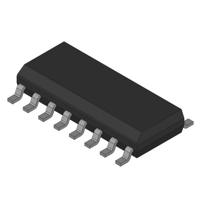
- Part No.:
- UCC3752DTR
- Manufacturer:
- Texas Instruments
- Category:
- Telecom
- Package:
- -
- Datasheet:
-
 UCC3752DTR.pdf
- Description:
- TELECOM CIRCUIT, 1-FUNC, BICMOS,
- Quantity:
- Payment:

- Shipping:

Inventory:2,500
Please send an inquiry. Send us your inquiry, and we will respond immediately.
Product details
Overview
UCC3752DTR from Texas Instruments is a resonant ring generator controller IC designed to drive push-pull primary switches and transformer-coupled sampling switches in telephone ringing circuits. It operates from a single 12V supply, delivers 1.5A pulsed output current on DRV1/DRV2/DRVS, supports selectable 20/25/50 Hz ring frequencies via FS0/FS1 pins, and integrates off-hook detection and primary current limiting for multi-line telephony systems.
For engineers reviewing the UCC3752DTR datasheet, UCC3752DTR pinout, UCC3752DTR application, or UCC3752DTR equivalent, this page provides verified technical context, validated pin functions, confirmed ring-frequency selectability, real-world off-hook detection behavior, and direct alternatives for legacy telephony power stage control.
Technical Context
The UCC3752DTR uses a fixed 3.579545 MHz crystal to derive precise primary switching (89.439–89.489 kHz) and secondary sampling frequencies, with frequency offset determined by FS0/FS1 logic states to generate 20/25/50 Hz alias output. Its internal architecture includes dual modulo counters, one-shot timers, and analog comparators for DCLIM and OHD threshold detection.
It implements cycle-by-cycle primary current limiting at 300 mV on DCLIM, off-hook detection at 300 mV on OHD with programmable pull-up/pull-down impedance, and generates 280 ns sampling pulses on DRVS for transformer-coupled secondary-side switching-enabling non-isolated, open-loop ring signal generation without feedback compensation.
Key Specifications
| Parameter | Value and Actual Design Meaning |
|---|---|
| Supply Voltage | 12 V DC input (VS12); supports operation up to 13.2 V absolute max. |
| Output Drive Current | 1.5 A pulsed per driver (DRV1, DRV2, DRVS); sufficient to directly drive gate of discrete MOSFETs in resonant converter. |
| Ringing Frequency Options | Selectable 20 Hz, 25 Hz, or 50 Hz via FS0/FS1 logic inputs; enables compliance with regional telephony standards. |
| DCLIM Threshold | 300 mV typical; triggers immediate shutdown of all outputs upon primary overcurrent detection. |
| OHD Threshold | 300 mV typical; initiates OFFHOOK flag assertion when secondary AC current exceeds limit. |
| VDD Output | 5.0 V ±150 mV regulated reference; powers internal precision circuitry and bypassed externally with ceramic capacitor. |
| Operating Temperature | 0°C to +70°C junction range; specified for commercial-grade telephony equipment environments. |
Pinout & Package
UCC3752DTR is housed in a 16-pin SOIC (D package), with exposed pad not present and thermal performance rated for continuous operation at ambient up to 70°C.
| Pin/Terminal | Circuit Role | Design Meaning |
|---|---|---|
| 1, 2, 3, 4, 5, 6, 7, 8, 9, 10, 11, 12, 13, 14, 15, 16 | Standard SOIC-16 pin mapping per TI SLUS269A | Pin numbering follows top-view DIL-16/SOIC-16 convention; exact function per pin defined below. |
| DRV1 / DRV2 | Complementary low-impedance gate drivers | Drive Q1/Q2 primary switches in push-pull configuration with 50% duty cycle and <100 ns rise/fall times. |
| DRVS | Sampling switch driver output | Generates 280 ns pulse at 89.439–89.489 kHz to trigger secondary-side sampling FET(s) via pulse transformer. |
| DCLIM | Primary current sense input | Monitors voltage across RSENSE; shuts down all outputs if ≥300 mV detected-cycle-by-cycle fault protection. |
| OHD | Off-hook detect input | Accepts AC-coupled secondary current signal; compares to 300 mV internal threshold to assert OFFHOOK flag. |
| OFFHOOK | Open-drain off-hook status output | Drives external logic or relay control; VOH = 4.0 V @ 1 mA, VOL = 1.5 V @ –1 mA, pull-up impedance 100–900 Ω. |
| FS0 / FS1 | Ring frequency select inputs | Hard-wired to GND/VDD to configure 20 Hz (00), 25 Hz (01), or 50 Hz (10); 11 reserved. |
| ENABLE | Active-high output enable | Disables all drivers when pulled low; allows system-level ring activation control. |
| VDD | Internal 5 V regulator output | Bypassed to GND with ceramic capacitor; supplies bias to internal analog/digital blocks. |
| VS12 | Main 12 V power input | Provides energy for driver outputs and powers internal LDO generating VDD. |
| PGND / GND | Power and signal ground returns | PGND is dedicated return for DRV1/DRV2/DRVS; GND is reference for analog/digital logic-connect at single point. |
| XTAL1 / XTAL2 | Crystal oscillator interface | Supports 3.579545 MHz fundamental-mode crystal; XTAL2 accepts external square wave if XTAL1 tied to VDD/2. |
| N/C | No-connect | Pin 2 has no internal connection; must remain unconnected. |
Key Features
| Feature | Design Value |
|---|---|
| Novel resonant ring topology | Enables low-cost, high-efficiency telephone ringing without isolation transformers or closed-loop regulation. |
| Selectable ring frequency | 20/25/50 Hz selection via two logic inputs meets global POTS line requirements without component changes. |
| Integrated off-hook detection | Direct AC current sensing on OHD pin eliminates need for external comparator or rectifier in line monitoring path. |
| Cycle-by-cycle current limiting | DCLIM input responds within one switching cycle to prevent MOSFET destruction during short-circuit or overload. |
| Single-supply operation | 12 V input powers both logic and gate drivers-reduces BOM count versus split-rail or multi-voltage solutions. |
Applications
| Central Office Line Card | Multi-Line VoIP Gateway |
|---|---|
|
Use Scenario: Generating standardized ringing voltage for up to five analog telephone lines in carrier-class line cards. IC Role / Device Role / Timing Role: Resonant ring generator controller coordinating primary switching and secondary sampling to produce 90 Vrms, 20 Hz sine-wave output. Use Value: Eliminates need for bulky isolation transformers and linear regulators while maintaining FCC Part 68 compliance for ring equivalence number (REN). |
Use Scenario: Providing PSTN-compatible ringing signals in enterprise VoIP gateways supporting 4–8 FXS ports. IC Role / Device Role / Timing Role: Timing-critical controller synchronizing 89.489 kHz primary drive and 89.469 kHz sampling to generate precise 20 Hz alias waveform. Use Value: Enables compact, low-power ring generation with minimal external components-critical for fanless, DIN-rail mounted gateways. |
| Hotel/Multi-Dwelling PBX | Emergency Alert System Terminal |
|
Use Scenario: Delivering simultaneous ringing to distributed analog extensions in hospitality or MDU telephone systems. IC Role / Device Role / Timing Role: Multi-line ring controller managing shared transformer resources and enabling staggered or grouped ring activation. Use Value: Supports up to five lines with consistent amplitude and frequency stability-ensuring reliable call delivery across long cable runs. |
Use Scenario: Powering emergency notification ringers in fire alarm panels or mass notification hardware requiring fail-safe AC ringing. IC Role / Device Role / Timing Role: Fault-tolerant ring generator with DCLIM-based shutdown and OFFHOOK flag for status reporting to supervisory MCU. Use Value: Provides built-in overcurrent and off-hook supervision-reducing firmware complexity and external monitoring circuitry. |
Equivalent & Alternatives
The following parts are listed as comparable options for similar resonant ring generator applications.
| Alternative Part | Technical Difference | Application Difference | Selection Advice |
|---|---|---|---|
| UCC3752N | Same die, PDIP-16 package; wider lead spacing, no moisture sensitivity rating. | Preferred for through-hole prototyping or legacy board rework where SOIC footprint unavailable. | Select UCC3752N only when manual assembly or socket-based testing is required; not suitable for automated SMT production. |
| UCC2752D | Extended temperature range (–40°C to +85°C); identical pinout and electrical specs except operating temp. | Required for outdoor or industrial telephony equipment exposed to extended ambient conditions. | Choose UCC2752D when deployment environment exceeds 70°C ambient or requires automotive-grade reliability screening. |
Compared with UCC3752DTR, UCC3752N offers mechanical compatibility for hand-soldered systems but lacks SOIC thermal performance, while UCC2752D adds industrial temperature support without altering timing, drive strength, or feature set-making it the drop-in upgrade for harsh environments.
Availability
UCC3752DTR is available at Aetrix Electronics and suitable for central office line cards, multi-line VoIP gateways, hotel PBX systems, and emergency alert terminals requiring stable component supply for legacy telephony infrastructure.
Supply support for UCC3752DTR includes scheduled delivery planning, volume procurement assistance, BOM continuity management, traceable sourcing, and lifecycle availability coordination for OEM customers, industrial embedded developers, connected-device designers, and electronics production programs.
Manufacturer
Texas Instruments is a global semiconductor company headquartered in Dallas, Texas, delivering analog, embedded processing, and connectivity technologies since 1930.
The UCC3752DTR belongs to TI's legacy telephony power management portfolio, engineered specifically for cost-sensitive, high-reliability ringing signal generation in analog line interface circuits.
FAQ
What is the primary function of the UCC3752DTR in a telephone ringing circuit?
The UCC3752DTR serves as a resonant ring generator controller that coordinates primary-side push-pull switching and secondary-side sampling to produce standardized low-frequency, high-voltage AC ringing signals. It directly drives external MOSFETs, manages frequency selection via FS0/FS1, and integrates off-hook detection and current limiting-enabling compact, efficient ring generation without isolation or feedback loops. The UCC3752DTR is optimized for multi-line POTS applications where cost, size, and reliability are critical.
Does the UCC3752DTR require an external crystal, and what frequency is needed?
Yes, the UCC3752DTR requires a 3.579545 MHz fundamental-mode crystal connected between XTAL1 and XTAL2 to establish precise timing for both primary switching and sampling frequencies. This crystal frequency is essential for achieving the specified 89.439–89.489 kHz switching range and accurate 20/25/50 Hz ring output offsets. An external square-wave clock may be applied to XTAL2 only if XTAL1 is biased at VDD/2, but crystal operation is the recommended and fully characterized method for UCC3752DTR.
How does the UCC3752DTR implement off-hook detection?
The UCC3752DTR implements off-hook detection using the OHD pin, which accepts an AC-coupled voltage proportional to secondary winding current. An internal 300 mV comparator monitors this signal; when exceeded, the open-drain OFFHOOK pin asserts high. The OFFHOOK output features programmable pull-up/pull-down impedance (100–900 Ω) and specified VOH/VOL levels, allowing direct interfacing with microcontrollers or logic supervisors. This integrated function replaces discrete op-amp or comparator circuits traditionally used for line supervision in UCC3752DTR-based designs.
Can the UCC3752DTR operate from a supply other than 12 V?
The UCC3752DTR is specified to operate from a nominal 12 V supply on VS12, with absolute maximum rating of 13.2 V. While the internal VDD regulator outputs 5 V for logic, the driver outputs (DRV1, DRV2, DRVS) derive their energy directly from VS12-so reducing VS12 below 12 V compromises peak output voltage swing and gate drive strength. Operation outside the 12 V ±10% range is not characterized, and deviation may cause waveform distortion or failure to meet ring voltage specifications. Therefore, UCC3752DTR must be powered from a stable 12 V source per its design intent.
What is the purpose of the DRVS pin on the UCC3752DTR?
The DRVS pin on the UCC3752DTR delivers precisely timed 280 ns sampling pulses at 89.439–89.489 kHz to drive secondary-side sampling switches-typically implemented with back-to-back FETs or a single FET plus full-bridge rectifier. These pulses are transformer-coupled to isolate the floating secondary circuit, enabling aliasing of the high-frequency transformer output into a low-frequency ringing waveform. The DRVS output has low-impedance drive capability (4–10 Ω pull-up/down) and fast edge rates (<100 ns), ensuring clean triggering of sampling devices in UCC3752DTR-based ring generators.
UCC3752DTR Specifications
- Product attributes
- Attribute value
- Manufacturer:
- Texas Instruments
- Series:
- *
- Package/Case:
- -
- Packaging:
- Bulk
- Product Status:
- Active
- Function:
- -
- Interface:
- -
- Number of Circuits:
- -
- Voltage - Supply:
- -
- Current - Supply:
- -
- Power (Watts):
- -
- Operating Temperature:
- -
- Grade:
- -
- Qualification:
- -
- Mounting Type:
- -
- Supplier Device Package:
- -
UCC3752DTR FAQ
1.How can I place an order for UCC3752DTR through Aetrix?
Please submit a Request for Quotation (RFQ) for UCC3752DTR on Aetrix. Our sales agent will provide a competitive quotation and guide you through the order confirmation once you accept the terms.
2.Are the price and stock information for UCC3752DTR reliable?
The price and inventory of UCC3752DTR are updated periodically and may fluctuate due to market conditions. Stock and pricing data are typically refreshed every 24 hours. Quotation validity for UCC3752DTR is usually 5 days.
3.What payment methods are accepted for UCC3752DTR?
We accept Wire Transfer, PayPal, Credit Card, Western Union, MoneyGram, and Escrow for UCC3752DTR transactions.
Note: Certain payment methods may incur a processing fee.
4.How is shipping managed for UCC3752DTR?
UCC3752DTR orders can be shipped via leading logistics carriers, including DHL, UPS, FedEx, TNT, or Registered Mail.
Once your UCC3752DTR order is processed, you will receive an email with the shipment details and tracking number.
Note: Tracking information may take up to 24 hours to appear. Express delivery typically takes 3–5 business days.
5.How can I obtain technical support or documentation for UCC3752DTR?
For technical support, including UCC3752DTR datasheets, pinout diagrams, or application guidance, please contact our engineering support team. They can provide detailed documentation and assistance for your UCC3752DTR requirements.
6.How does Aetrix verify that UCC3752DTR is sourced from the original manufacturer or authorized distributors?
All UCC3752DTR products on Aetrix are procured from qualified distributors and authorized channels. Our dedicated quality assurance team conducts strict verification, including traceability checks and, if necessary, third-party testing. This ensures that UCC3752DTR meets industry standards.
7.What is the process for return or replacement of UCC3752DTR?
All UCC3752DTR units undergo pre-shipment inspection (PSI). If there is an issue with UCC3752DTR, returns or replacements are accepted under the following conditions:
1.Quantity discrepancies, incorrect items, or visible external defects (such as breakage or corrosion), acknowledged by Aetrix.
2.The issue is reported within 90 days of delivery.
3.The UCC3752DTR part is unused and in its original packaging.
Return procedure for UCC3752DTR:
1.Submit a request within 90 days.
2.Obtain a Return Material Authorization (RMA) from Aetrix.
UCC3752DTR Tags

-
LMC567CMX/NOPB
Texas Instruments
-
LM567CMX/NOPB
Texas Instruments
-
LM567CM/NOPB
Texas Instruments

-
VSC8531XMW-02
Microchip Technology
-
VSC8531XMW-05
Microchip Technology

-
GPY115C0VI
MaxLinear, Inc.

-
SI32185-A-FMR
Skyworks Solutions Inc.

-
VSC8541XMV-05
Microchip Technology

-
SI32178-B-FM1R
Skyworks Solutions Inc.
-
GPY215C0VI
MaxLinear, Inc.

-
CPC7514ZTR
Littelfuse Inc.

-
VSC8502XML-03
Microchip Technology
Tech Hub

A practical engineering guide to 3.3V and 5V logic compatibility, input thresholds, resistor dividers, translator ICs, MOSFET level shifting, I2C pull-ups, timing limits and power-sequencing risks.

The 74HC595 uses push-pull logic outputs, while the TPIC6B595 uses 50 V open-drain DMOS sinks for higher-power loads. This guide compares timing, current limits, 3.3 V interfacing, load wiring, thermal…

The 74HC595 converts serial data into eight stable parallel outputs. This guide covers pin functions, shift and storage timing, OE and MR behavior, drive-current limits, cascading, voltage compatibilit…

A technical comparison of level-sensitive latches and edge-triggered flip-flops, covering timing windows, setup and hold limits, master–slave operation, time borrowing, race-through, HDL inference and…

A D latch stores one bit while Enable controls when data can pass. This reference covers gate-level operation, truth tables, transparency, setup and hold timing, LE versus OE, common ICs and practical …

An SR latch stores one bit through cross-coupled feedback. This engineering reference covers NOR and NAND implementations, truth tables, forbidden-state recovery, gated operation, switch debouncing, fa…

Latch circuits retain one bit through feedback. This technical reference covers SR and D latches, truth tables, transparency, timing limits, latch-versus-flip-flop behavior, applications and common log…

An engineering guide to LED driver operation, constant-current and constant-voltage outputs, linear and switching topologies, dimming, IC selection, calculations, replacement compatibility, and fault c…

Operational amplifier guide covering op amp basics, feedback, ideal vs real op amps, common configurations, buffer circuits, offset, bias current, gain-bandwidth, slew rate, rail-to-rail limits and sel…

Jumper cables guide covering safe connection order, red and black clamp placement, final ground connection, cable gauge, length, clamp quality, copper vs CCA cables, jump starter comparison and battery…


