
 My Inquiry
 My Account


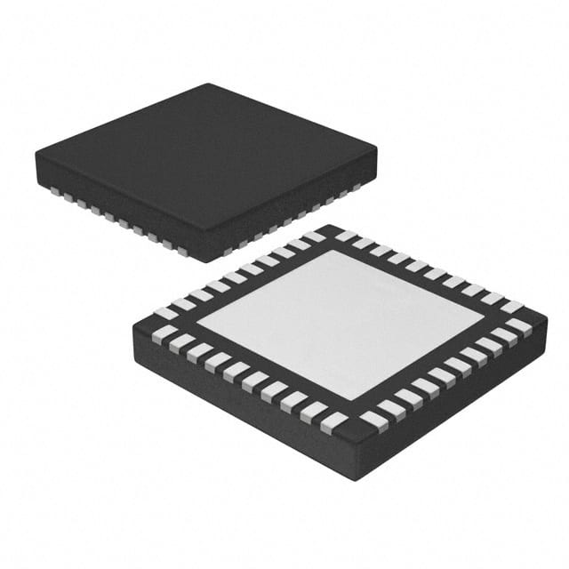
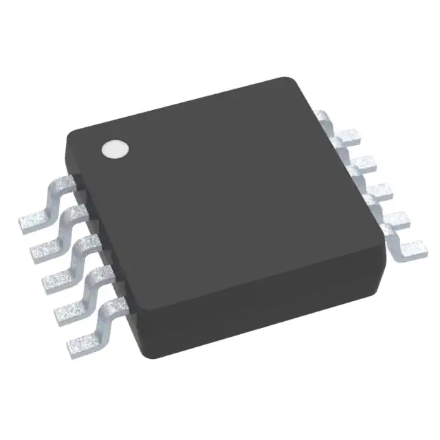
Texas Instruments UCD3138RHAR
- Part No.:
- UCD3138RHAR
- Manufacturer:
- Texas Instruments
- Category:
- Power Supply Controllers, Monitors
- Package:
- 40-VFQFN Exposed Pad
- Datasheet:
-
 UCD3138RHAR.pdf
- Description:
- IC DGTL PWR CTRLR 40VQFN
- Quantity:
- Payment:

- Shipping:

Inventory:2,454
Please send an inquiry. Send us your inquiry, and we will respond immediately.
Product details
Overview
UCD3138RHAR from Texas Instruments is a highly integrated digital power controller for isolated DC-DC and AC-DC applications, featuring three independent PID-based digital control loops, 8 high-resolution DPWM outputs with 250-ps pulse width resolution, and a 31.25 MHz ARM7TDMI-S processor with 32 KB flash and 4 KB RAM. It supports voltage, peak/average current, constant current, and constant power modes for telecom rectifiers and PFC stages.
For engineers reviewing the UCD3138RHAR datasheet, UCD3138RHAR pinout, UCD3138RHAR application, or UCD3138RHAR equivalent, key selection criteria include DPWM timing resolution (4 ns frequency/phase), EADC resolution (as low as 1 mV/LSB), burst mode and ideal diode emulation for light-load efficiency, and support for phase-shifted full-bridge, LLC, and dual-phase PFC topologies.
Technical Context
The UCD3138RHAR implements three dedicated Digital Power Peripherals (DPPs), each integrating an error ADC, configurable 2-pole/2-zero digital compensator, and hardware-accelerated loop execution - enabling sub-microsecond closed-loop response. Its DPWM module delivers cycle-by-cycle duty matching and adjustable dead-band between complementary pairs, critical for ZVS/ZCS soft-switching in resonant converters.
It integrates a 12-bit, 267-ksps general-purpose ADC with programmable averaging filters and dual sample-and-hold, plus seven high-speed analog comparators with blanking and fault counting - all synchronized to the ARM core's real-time firmware for adaptive protection and dynamic mode switching between PWM, phase-shift, and frequency modulation.
Key Specifications
| Parameter | Value and Actual Design Meaning |
|---|---|
| DPWM Resolution | 250-ps pulse width resolution enables precise timing control for ZVS optimization in LLC and PSFB topologies. |
| EADC Resolution | Configurable down to 1 mV/LSB with automatic selection - supports accurate voltage regulation across wide output ranges. |
| Control Loops | 3 independent hardware PID loops with nonlinear control and adaptive sample trigger positioning for fast transient response. |
| Processor Core | 31.25 MHz ARM7TDMI-S with 32 KB flash, 4 KB RAM, and boot ROM - executes real-time monitoring and communication without external host. |
| ADC Channels | 14 external + 1 internal temperature channel at 267 ksps - sufficient for multi-sensor feedback in modular PSUs. |
| Operating Temp | –40°C to 125°C ambient - qualified for industrial and telecom infrastructure environments with extended thermal margin. |
| Switching Freq | Up to 2 MHz DPWM operation - supports high-frequency GaN/SiC designs while maintaining resolution and stability. |
Pinout & Package
VQFN-40 package (6.00 mm × 6.00 mm) with exposed thermal pad; RoHS-compliant, lead-free finish; 0.5-mm pitch; designed for high-power density layouts with optimized thermal dissipation.
| Pin/Terminal | Circuit Role | Design Meaning |
|---|---|---|
| DPWM0A / DPWM0B | Complementary DPWM output pair | Drives high-side/low-side switches in half-bridge; supports adjustable dead-band and phase shift for ZVS tuning. |
| EAP0 / EAN0 | Error amplifier input (loop 0) | Differential analog input for primary-side voltage or current sensing; feeds dedicated EADC with 1-mV/LSB resolution. |
| AD00–AD02 | General-purpose ADC inputs | Monitor auxiliary voltages, temperatures, or current-share bus; support copper trace sensing and flux balancing. |
| FAULT0 / FAULT1 / FAULT2 | Dedicated fault inputs | Accept fast overcurrent/overvoltage signals with programmable blanking and cycle-by-cycle limiting. |
| PMBUS_DATA / PMBUS_CLK | PMBus v1.2 interface | Enables real-time telemetry, configuration, and fault logging via industry-standard power management bus. |
| /RESET | Active-low reset input | Hardware reset with external RC timing control per TI design guidelines for robust power sequencing. |
| AGND / DGND | Analog & digital ground pins | Separate ground domains minimize noise coupling between sensitive analog front-end and high-speed DPWM logic. |
Key Features
| Feature | Design Value |
|---|---|
| Hardware PID Compensator | Three independent, fully configurable 2-pole/2-zero digital filters execute in dedicated hardware - no CPU overhead, deterministic latency <1 µs. |
| Burst Mode & Ideal Diode Emulation | Reduces standby power and improves light-load efficiency in isolated DC-DC modules without external circuitry. |
| Synchronous Rectifier Soft On/Off | Prevents shoot-through and reduces EMI during gate transitions - critical for high-efficiency secondary-side control. |
| Current Share Bus Support | Analog average or master/slave topology enables precise load balancing across parallel power stages without external op-amps. |
| Fusion Digital Power Studio GUI | Real-time parameter tuning, waveform capture, and firmware update via USB-to-PMBus adapter - accelerates lab validation and field calibration. |
Applications
| Telecom Rectifier | Server PSU |
|---|---|
Use Scenario: 48 V input, 12 V/54 A output telecom rectifier operating at 96% efficiency with dynamic load steps up to 50 A/µs. IC Role / Device Role / Timing Role: Primary-side digital controller managing phase-shifted full-bridge topology with synchronous rectification and input voltage feed-forward. Use Value: Hardware-accelerated burst mode and ideal diode emulation maintain >90% efficiency at 5% load; 250-ps DPWM resolution ensures precise ZVS timing across line/load variations. | Use Scenario: Dual-output (12 V/54 A, 3.3 V/20 A) server PSU with active current sharing between parallel modules. IC Role / Device Role / Timing Role: Master controller coordinating three independent regulation loops and analog-average current share bus across redundant units. Use Value: Cycle-by-cycle duty matching and programmable fault counting enable seamless hot-swap and graceful degradation under single-point failures. |
| PFC Front-End | Isolated DC-DC Module |
Use Scenario: Bridgeless totem-pole PFC stage delivering 3.5 kW at PF >0.99 with THD <5% across universal AC input. IC Role / Device Role / Timing Role: Constant-power control loop with copper trace current sensing and adaptive sample trigger positioning for fast line transients. Use Value: Peak current mode control on EADC2 enables stable operation at >200 kHz switching with minimal external components. | Use Scenario: 400 V input, 12 V/60 A isolated DC-DC module using LLC resonant topology in data center power shelves. IC Role / Device Role / Timing Role: Dual-loop controller regulating both primary-side resonant frequency and secondary-side synchronous rectifier timing. Use Value: Hardware-based phase-shift modulation and 4-ns phase resolution allow fine-grained tuning of zero-voltage switching window across temperature and aging. |
Equivalent & Alternatives
The following parts are listed as comparable options for similar digital power controller applications.
| Alternative Part | Technical Difference | Application Difference | Selection Advice |
|---|---|---|---|
| UCD3138RGC | 64-pin QFN with 2 UARTs, 14 ADC channels, and additional GPIOs; same core architecture and DPWM specs. | Required for designs needing dual UARTs, higher ADC channel count, or more flexible pin multiplexing (e.g., timer capture + SCI + PMBus). | Select RGC when system-level I/O expansion or debug capability (JTAG + SCI) is required beyond RHA's footprint-constrained layout. |
| UCD3138A64PFC | Optimized PFC variant with enhanced front-end for bridgeless/totem-pole topologies; includes dedicated PFC firmware libraries and modified EADC biasing. | Targeted specifically at high-power PFC stages; lacks full 3-loop flexibility and secondary-side SR control features of UCD3138RHAR. | Choose A64PFC only for dedicated front-end PFC controllers where isolated DC-DC regulation is handled by separate ICs. |
Compared with UCD3138RGC, the UCD3138RHAR offers identical control loop performance and DPWM resolution in a smaller 40-pin package but trades off UART count and ADC channel count - making it optimal for space-constrained, cost-sensitive isolated DC-DC modules. Against UCD3138A64PFC, it provides broader topology support and full firmware programmability at the expense of PFC-specific analog enhancements.
Availability
UCD3138RHAR is available at Aetrix Electronics and suitable for telecom rectifiers, server PSUs, and isolated DC-DC modules requiring stable component supply, long-term lifecycle assurance, and production-ready qualification for industrial temperature operation.
Supply support for UCD3138RHAR includes scheduled delivery planning, volume procurement assistance, BOM continuity management, traceable sourcing, and lifecycle availability coordination for OEM customers, industrial embedded developers, connected-device designers, and electronics production programs.
Manufacturer
Texas Instruments is a global semiconductor leader specializing in analog, embedded processing, and power management technologies, with decades of expertise in digital power control and energy-efficient system solutions.
The UCD3138 family was developed to replace analog controllers in high-performance isolated power supplies, delivering programmable flexibility, hardware-accelerated control loops, and integrated PMBus telemetry for next-generation data center and telecom infrastructure.
FAQ
What is the maximum DPWM switching frequency supported by the UCD3138RHAR?
The UCD3138RHAR supports DPWM operation up to 2 MHz. This specification is validated across the full –40°C to 125°C operating temperature range and enables compatibility with GaN and high-frequency SiC MOSFETs in resonant and hard-switched topologies. The 4-ns frequency resolution ensures precise timing control even at maximum switching rates, and the hardware-based cycle-by-cycle duty matching maintains symmetry under dynamic load conditions. All UCD3138RHAR units shipped meet this spec per TI's production test flow.
Does the UCD3138RHAR support peak current mode control?
Yes, the UCD3138RHAR supports peak current mode control using its dedicated EADC2 front-end, which is optimized for fast current sensing with adaptive blanking and comparator-based cycle-by-cycle limiting. Unlike generic ADC channels, EADC2 provides hardware-triggered sampling aligned to DPWM edges, enabling stable operation at >200 kHz with minimal external components. This capability is explicitly documented in the UCD3138RHAR datasheet Section 9.5 and confirmed in TI Application Report SLUA902.
How many independent feedback loops does the UCD3138RHAR implement, and are they fully configurable?
The UCD3138RHAR implements three independent, hardware-accelerated digital feedback loops - each with a dedicated EADC, configurable 2-pole/2-zero PID filter, and associated DPWM outputs. All loops support voltage mode, peak/average current mode, constant current, and constant power configurations via firmware registers. Loop parameters (gain, zero/pole locations, sample rate) are fully programmable in real time without CPU intervention, and nonlinear control features like burst mode and soft-start are applied per-loop. This architecture is detailed in the UCD3138RHAR Technical Reference Manual (SPRUH17).
What communication interfaces are available on the UCD3138RHAR?
UCD3138RHAR provides one PMBus/I²C interface and one UART (SCI) interface. The PMBus interface supports full v1.2 command set for telemetry, configuration, and fault logging; the UART supports asynchronous serial communication for firmware updates and debug. Unlike the 64-pin RGC variant, the 40-pin RHAR does not include a second UART. Both interfaces operate at 3.3-V logic levels and are electrically isolated from DPWM domains per TI's layout recommendations in SLUU375.
Is the UCD3138RHAR pin-compatible with other members of the UCD3138 family?
No, the UCD3138RHAR is not pin-compatible with UCD3138RGC (64-pin) or UCD3138RJA (40-pin with corner anchors). While all share the same functional blocks and register map, the RHAR uses a 40-pin VQFN package with specific pin assignments - including consolidated fault inputs and shared PMBus/UART pins - that differ from RGC's expanded I/O and RJA's mechanical anchor layout. Migration requires PCB redesign; however, firmware is binary-compatible across the family when using TI's Fusion Digital Power Designer software.
UCD3138RHAR Specifications
- Product attributes
- Attribute value
- Manufacturer:
- Texas Instruments
- Series:
- -
- Package/Case:
- 40-VFQFN Exposed Pad
- Packaging:
- Tape & Reel (TR)
- Product Status:
- Active
- Programmable:
- Not Verified
- Applications:
- Digital Power Controller
- Voltage - Input:
- -
- Voltage - Supply:
- 3V ~ 3.6V
- Current - Supply:
- 100 mA
- Operating Temperature:
- -40°C ~ 125°C
- Grade:
- -
- Qualification:
- -
- Mounting Type:
- Surface Mount
- Supplier Device Package:
- 40-VQFN (6x6)
UCD3138RHAR FAQ
1.How can I place an order for UCD3138RHAR through Aetrix?
Please submit a Request for Quotation (RFQ) for UCD3138RHAR on Aetrix. Our sales agent will provide a competitive quotation and guide you through the order confirmation once you accept the terms.
2.Are the price and stock information for UCD3138RHAR reliable?
The price and inventory of UCD3138RHAR are updated periodically and may fluctuate due to market conditions. Stock and pricing data are typically refreshed every 24 hours. Quotation validity for UCD3138RHAR is usually 5 days.
3.What payment methods are accepted for UCD3138RHAR?
We accept Wire Transfer, PayPal, Credit Card, Western Union, MoneyGram, and Escrow for UCD3138RHAR transactions.
Note: Certain payment methods may incur a processing fee.
4.How is shipping managed for UCD3138RHAR?
UCD3138RHAR orders can be shipped via leading logistics carriers, including DHL, UPS, FedEx, TNT, or Registered Mail.
Once your UCD3138RHAR order is processed, you will receive an email with the shipment details and tracking number.
Note: Tracking information may take up to 24 hours to appear. Express delivery typically takes 3–5 business days.
5.How can I obtain technical support or documentation for UCD3138RHAR?
For technical support, including UCD3138RHAR datasheets, pinout diagrams, or application guidance, please contact our engineering support team. They can provide detailed documentation and assistance for your UCD3138RHAR requirements.
6.How does Aetrix verify that UCD3138RHAR is sourced from the original manufacturer or authorized distributors?
All UCD3138RHAR products on Aetrix are procured from qualified distributors and authorized channels. Our dedicated quality assurance team conducts strict verification, including traceability checks and, if necessary, third-party testing. This ensures that UCD3138RHAR meets industry standards.
7.What is the process for return or replacement of UCD3138RHAR?
All UCD3138RHAR units undergo pre-shipment inspection (PSI). If there is an issue with UCD3138RHAR, returns or replacements are accepted under the following conditions:
1.Quantity discrepancies, incorrect items, or visible external defects (such as breakage or corrosion), acknowledged by Aetrix.
2.The issue is reported within 90 days of delivery.
3.The UCD3138RHAR part is unused and in its original packaging.
Return procedure for UCD3138RHAR:
1.Submit a request within 90 days.
2.Obtain a Return Material Authorization (RMA) from Aetrix.
UCD3138RHAR Tags

-
UC3845AD8TR
Texas Instruments
-
UC2843AD8TR
Texas Instruments

-
LM3880MFX-1AE/NOPB
Texas Instruments
-
LM3880MFX-1AA/NOPB
Texas Instruments
-
INA234AIYBJR
Texas Instruments

-
INA700AYWFR
Texas Instruments
-
LM3880MF-1AE/NOPB
Texas Instruments
-
LM3880MF-1AA/NOPB
Texas Instruments
-
LM3881MM/NOPB
Texas Instruments
-
UCC2802DTR
Texas Instruments
-
NCP4305DMTTWG
onsemi
-
INA237AIDGSR
Texas Instruments
Tech Hub

A practical engineering guide to 3.3V and 5V logic compatibility, input thresholds, resistor dividers, translator ICs, MOSFET level shifting, I2C pull-ups, timing limits and power-sequencing risks.

The 74HC595 uses push-pull logic outputs, while the TPIC6B595 uses 50 V open-drain DMOS sinks for higher-power loads. This guide compares timing, current limits, 3.3 V interfacing, load wiring, thermal…

The 74HC595 converts serial data into eight stable parallel outputs. This guide covers pin functions, shift and storage timing, OE and MR behavior, drive-current limits, cascading, voltage compatibilit…

A technical comparison of level-sensitive latches and edge-triggered flip-flops, covering timing windows, setup and hold limits, master–slave operation, time borrowing, race-through, HDL inference and…

A D latch stores one bit while Enable controls when data can pass. This reference covers gate-level operation, truth tables, transparency, setup and hold timing, LE versus OE, common ICs and practical …

An SR latch stores one bit through cross-coupled feedback. This engineering reference covers NOR and NAND implementations, truth tables, forbidden-state recovery, gated operation, switch debouncing, fa…

Latch circuits retain one bit through feedback. This technical reference covers SR and D latches, truth tables, transparency, timing limits, latch-versus-flip-flop behavior, applications and common log…

An engineering guide to LED driver operation, constant-current and constant-voltage outputs, linear and switching topologies, dimming, IC selection, calculations, replacement compatibility, and fault c…

Operational amplifier guide covering op amp basics, feedback, ideal vs real op amps, common configurations, buffer circuits, offset, bias current, gain-bandwidth, slew rate, rail-to-rail limits and sel…

Jumper cables guide covering safe connection order, red and black clamp placement, final ground connection, cable gauge, length, clamp quality, copper vs CCA cables, jump starter comparison and battery…


