
 My Inquiry
 My Account


NXP Semiconductors UDA1345TS/N2,118
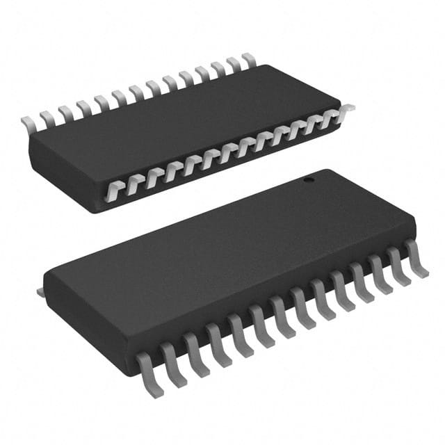
- Part No.:
- UDA1345TS/N2,118
- Manufacturer:
- NXP Semiconductors
- Category:
- CODECS
- Package:
- 28-SSOP (0.209", 5.30mm Width)
- Datasheet:
-
 UDA1345TS/N2,118.pdf
- Description:
- IC AUDIO CODED 24BIT 28SSOP
- Quantity:
- Payment:

- Shipping:

Inventory:4,564
Please send an inquiry. Send us your inquiry, and we will respond immediately.
Product details
Overview
UDA1345TS/N2,118 from NXP Semiconductors is a low-power stereo audio CODEC integrating sigma-delta ADC and DAC with digital interpolation/decimation filters, 2.4–3.6 V supply operation, 8–100 kHz sampling support, and dual control modes (L3 microcontroller or static pins). It delivers 96 dB SNR (ADC), 100 dB SNR (DAC), and −85 dB THD+N at 44.1 kHz for portable digital audio record/playback systems.
For engineers reviewing the UDA1345TS/N2,118 datasheet, UDA1345TS/N2,118 pinout, UDA1345TS/N2,118 application, or UDA1345TS/N2,118 equivalent, key selection criteria include its 28-pin SSOP package, I²S/MSB/LSB interface compatibility up to 24 bits, L3-controlled digital volume/de-emphasis/soft mute, and absence of bass-boost/treble features compared to UDA1344TS.
Technical Context
The UDA1345TS/N2,118 implements a 5th-order sigma-delta ADC with 64× oversampling and a 3rd-order noise-shaping DAC operating at 128fs, both using bitstream conversion. Its decimation filter achieves 114 dB dynamic range (ADC) and interpolation filter provides 116.5 dB (DAC), with inherent DC cancellation and overload detection.
Control is supported in two mutually exclusive modes: L3 microcontroller interface (8-bit address/data transfers, register-based configuration of clock, format, volume, de-emphasis, mute, power, and DC filter) or static pin mode (MP2/MP3/MP4/MP5 direct logic-level configuration of mute, de-emphasis, system clock, gain, and data format).
Key Specifications
| Parameter | Value and Actual Design Meaning |
|---|---|
| Supply Voltage | 2.4–3.6 V analog/digital rails; enables battery-powered operation with 3.0 V typical |
| Sampling Rate | 8–100 kHz; supports double-speed playback (e.g., 88.2/96 kHz) via 512fs clock mode |
| SNR (ADC) | 96 dB A-weighted at 44.1 kHz; defines minimum detectable signal level in recording path |
| SNR (DAC) | 100 dB A-weighted at 44.1 kHz; ensures high-fidelity line output without external filtering |
| THD+N | −85 dB at 0 dBFS, 44.1 kHz; specifies distortion/noise floor during full-scale playback |
| Interface Formats | I²S, MSB-justified (≤24 bits), LSB-justified (16/18/20 bits); enables interoperability with diverse SoCs and DSPs |
| Power Consumption | 64 mW (record+playback), 2.2 mW (power-down); critical for thermal management in compact enclosures |
Pinout & Package
UDA1345TS/N2,118 is housed in a plastic shrink small outline package (SSOP28) with 28 leads and 5.3 mm body width (SOT341-1), optimized for surface-mount assembly and space-constrained portable designs.
| Pin/Terminal | Circuit Role | Design Meaning |
|---|---|---|
| VSSA(ADC) (1) | ADC analog ground | Reference return for left/right analog inputs; must be isolated from digital ground to minimize coupling |
| VDDA(ADC) (2) | ADC analog supply | Provides regulated 2.4–3.6 V to ADC core; decoupling capacitor required near pin |
| VINL/VINR (3,5) | Stereo analog input | Accepts 1 V or 2 V RMS signals; gain selection (0/6 dB) configured via MP4 (static) or MP5 (L3) |
| SYSCLK (12) | System clock input | Accepts 256fs/384fs/512fs master clock; frequency locked to WS/BCK for synchronous audio transfer |
| BCK/WS/DATAI/DATAO (16–19) | Digital audio interface | Supports I²S/MSB/LSB formats; BCK ≤128×WS required; WS edge must align to BCK falling edge |
| MP1–MP5 (9,13–15,20) | Multi-purpose control | Configurable as OVERFL output, L3 interface lines, or static-mode gain/mute/de-emphasis selectors |
| VOUTL/VOUTR (26,24) | Stereo line output | DC-coupled outputs capable of 900 mV RMS into 5 kΩ; no external post-filter needed due to FSDAC architecture |
Key Features
| Feature | Design Value |
|---|---|
| Filter Stream DAC (FSDAC) | Current-source-based semi-digital reconstruction eliminates need for external analog filters and reduces jitter sensitivity |
| Digital DC Cancellation Filter | Configurable IIR high-pass filter removes offset drift without analog components or calibration |
| L3 Microcontroller Interface | 8-bit serial bus enables dynamic control of volume (1 dB steps), de-emphasis (32/44.1/48 kHz), and soft mute (cosine roll-off) |
| Overload Detection | Dedicated OVERFL pin asserts HIGH for ≥512fs cycles when digital output exceeds −1.16 dBFS, enabling automatic AGC in record path |
| Static Pin Mode | Hardware-configurable operation without MCU; MP2/MP3/MP4 set mute, de-emphasis, clock, and gain via logic levels |
Applications
| Portable MP3 Player | Digital Voice Recorder |
|---|---|
Use Scenario: Battery-powered handheld device performing simultaneous audio playback and voice memo recording. IC Role / Device Role / Timing Role: Single-chip stereo CODEC handling analog input conditioning, sigma-delta conversion, digital filtering, and line-level output drive. Use Value: 64 mW total power enables >10-hour playback on single-cell Li-ion; 96 dB SNR ensures clean recording even in noisy environments. | Use Scenario: Compact office recorder capturing meetings with adjustable input gain and automatic level control. IC Role / Device Role / Timing Role: ADC front-end with overload detection and DC cancellation, plus DAC for monitoring playback through headphones. Use Value: OVERFL pin triggers firmware AGC; 2 V RMS input support with 12 kΩ series resistor accommodates line-level sources without attenuation. |
| USB Audio Adapter | Embedded Set-Top Box Audio |
Use Scenario: PC peripheral converting USB audio streams to analog line-out for powered speakers. IC Role / Device Role / Timing Role: Slave-mode DAC receiving I²S data from USB bridge IC; L3 interface configures de-emphasis and volume. Use Value: 100 dB SNR and −85 dB THD+N meet consumer audio fidelity requirements; 5 V-tolerant digital inputs simplify level-shifting with USB controller. | Use Scenario: Low-cost STB with HDMI/SPDIF input and analog stereo output for legacy AV receivers. IC Role / Device Role / Timing Role: Playback-only DAC processing SPDIF-derived I²S; static pin mode sets fixed 44.1 kHz de-emphasis and mute behavior. Use Value: Eliminates need for external microcontroller; 2.4–3.6 V operation allows direct connection to STB's 3.3 V rail, reducing BOM count. |
Equivalent & Alternatives
The following parts are listed as comparable options for similar audio CODEC applications.
| Alternative Part | Technical Difference | Application Difference | Selection Advice |
|---|---|---|---|
| UDA1344TS/N2,118 | Pin/function compatible but includes bass-boost and treble tone controls; otherwise identical ADC/DAC specs and pinout | Required where analog EQ is needed in playback path; not drop-in if tone controls unused | Select UDA1344TS/N2,118 only if bass/treble adjustment is mandatory; UDA1345TS/N2,118 preferred for minimal feature set and lower cost |
| AK4537VN | 24-bit stereo CODEC with 98 dB SNR (DAC), 3.3 V only supply, SPI/I²S interface, no static pin mode | Requires MCU for all configuration; higher SNR but lacks hardware-configurable modes and overload detection | Choose AK4537VN for higher fidelity and SPI compatibility; UDA1345TS/N2,118 better for MCU-less designs or AGC-driven record systems |
Compared with UDA1344TS/N2,118, the UDA1345TS/N2,118 removes tone controls while retaining identical power, SNR, and interface flexibility-making it optimal for cost-sensitive, feature-minimal audio paths. Versus AK4537VN, it trades 2 dB SNR for static-mode configurability and integrated overload signaling.
Availability
UDA1345TS/N2,118 is available at Aetrix Electronics and suitable for portable audio players, digital voice recorders, USB audio adapters, and embedded set-top boxes requiring stable component supply across production lifecycles.
Supply support for UDA1345TS/N2,118 includes scheduled delivery planning, volume procurement assistance, BOM continuity management, traceable sourcing, and lifecycle availability coordination for OEM customers, industrial embedded developers, connected-device designers, and electronics production programs.
Manufacturer
NXP Semiconductors is a global semiconductor company headquartered in Eindhoven, Netherlands, specializing in secure connectivity solutions for automotive, industrial, and consumer electronics.
The UDA1345TS/N2,118 belongs to NXP's economy audio CODEC product line, designed specifically for cost-optimized, low-power portable digital audio devices requiring integrated ADC/DAC functionality without premium signal processing features.
FAQ
What is the maximum input voltage supported by the UDA1345TS/N2,118 ADC?
The UDA1345TS/N2,118 ADC accepts up to 2 V (RMS) input voltage when a 12 kΩ series resistor is used to limit current to ~1 mA. Without the resistor, maximum input is 1 V (RMS) at 3 V supply. Input voltage scales proportionally with VDDA(ADC), so at 2.4 V supply, max input is ~0.8 V (RMS) without resistor. The UDA1345TS/N2,118 datasheet specifies this in Section 7.2 and Table 1.
Does the UDA1345TS/N2,118 support 192 kHz sampling rates?
No, the UDA1345TS/N2,118 supports sampling frequencies from 8 kHz to 100 kHz. In 512fs clock mode, the upper limit is reduced to 55 kHz. It does not support 192 kHz operation, as confirmed in Section 7 and Quick Reference Data. The UDA1345TS/N2,118 is designed for standard CD-quality (44.1 kHz) and DVD-audio (96 kHz) applications, not high-resolution studio sampling.
Can the UDA1345TS/N2,118 operate without a microcontroller?
Yes, the UDA1345TS/N2,118 supports static pin mode where MC1 and MC2 are both held HIGH. In this mode, functions like mute, de-emphasis, system clock selection, and ADC gain are controlled directly via MP2, MP3, and MP4 logic levels-eliminating MCU dependency. This is documented in Section 7.11 and Table 8–11 of the UDA1345TS/N2,118 datasheet.
What is the purpose of the OVERFL pin on the UDA1345TS/N2,118?
Pin 9 (MP1) serves as the OVERFL (overload flag) output in L3 mode. It asserts HIGH for at least 512fs cycles whenever the ADC digital output exceeds −1.16 dBFS in either channel, enabling real-time automatic gain control in recording applications. This behavior is defined in Section 7.10.5 and applies only when MC1/MC2 are LOW. The UDA1345TS/N2,118 uses this signal to prevent clipping without requiring host processor intervention.
Is the UDA1345TS/N2,118 pin-compatible with other UDA13xx devices?
The UDA1345TS/N2,118 is pin and function compatible with the UDA1344TS, as explicitly stated in Section 1.1 of the datasheet. However, it is not compatible with UDA1340M in static pin mode due to differing pin assignments (e.g., MP1 role differs), and lacks bass-boost/treble present in UDA1344TS. Always verify mode-specific pin definitions in Tables 5 and 7 before substitution. The UDA1345TS/N2,118 maintains mechanical and electrical compatibility only with UDA1344TS.
UDA1345TS/N2,118 Specifications
- Product attributes
- Attribute value
- Manufacturer:
- NXP Semiconductors
- Series:
- -
- Package/Case:
- 28-SSOP (0.209", 5.30mm Width)
- Packaging:
- Tape & Reel (TR)
- Product Status:
- Obsolete
- Type:
- Stereo Audio
- Data Interface:
- Serial
- Resolution (Bits):
- 24 b
- Number of ADCs / DACs:
- 2 / 2
- Sigma Delta:
- Yes
- S/N Ratio, ADCs / DACs (db) Typ:
- 96 / 100
- Dynamic Range, ADCs / DACs (db) Typ:
- -
- Voltage - Supply, Analog:
- 2.4V ~ 3.6V
- Voltage - Supply, Digital:
- 2.4V ~ 3.6V
- Operating Temperature:
- -40°C ~ 85°C
- Grade:
- -
- Qualification:
- -
- Mounting Type:
- Surface Mount
- Supplier Device Package:
- 28-SSOP
UDA1345TS/N2,118 FAQ
1.How can I place an order for UDA1345TS/N2,118 through Aetrix?
Please submit a Request for Quotation (RFQ) for UDA1345TS/N2,118 on Aetrix. Our sales agent will provide a competitive quotation and guide you through the order confirmation once you accept the terms.
2.Are the price and stock information for UDA1345TS/N2,118 reliable?
The price and inventory of UDA1345TS/N2,118 are updated periodically and may fluctuate due to market conditions. Stock and pricing data are typically refreshed every 24 hours. Quotation validity for UDA1345TS/N2,118 is usually 5 days.
3.What payment methods are accepted for UDA1345TS/N2,118?
We accept Wire Transfer, PayPal, Credit Card, Western Union, MoneyGram, and Escrow for UDA1345TS/N2,118 transactions.
Note: Certain payment methods may incur a processing fee.
4.How is shipping managed for UDA1345TS/N2,118?
UDA1345TS/N2,118 orders can be shipped via leading logistics carriers, including DHL, UPS, FedEx, TNT, or Registered Mail.
Once your UDA1345TS/N2,118 order is processed, you will receive an email with the shipment details and tracking number.
Note: Tracking information may take up to 24 hours to appear. Express delivery typically takes 3–5 business days.
5.How can I obtain technical support or documentation for UDA1345TS/N2,118?
For technical support, including UDA1345TS/N2,118 datasheets, pinout diagrams, or application guidance, please contact our engineering support team. They can provide detailed documentation and assistance for your UDA1345TS/N2,118 requirements.
6.How does Aetrix verify that UDA1345TS/N2,118 is sourced from the original manufacturer or authorized distributors?
All UDA1345TS/N2,118 products on Aetrix are procured from qualified distributors and authorized channels. Our dedicated quality assurance team conducts strict verification, including traceability checks and, if necessary, third-party testing. This ensures that UDA1345TS/N2,118 meets industry standards.
7.What is the process for return or replacement of UDA1345TS/N2,118?
All UDA1345TS/N2,118 units undergo pre-shipment inspection (PSI). If there is an issue with UDA1345TS/N2,118, returns or replacements are accepted under the following conditions:
1.Quantity discrepancies, incorrect items, or visible external defects (such as breakage or corrosion), acknowledged by Aetrix.
2.The issue is reported within 90 days of delivery.
3.The UDA1345TS/N2,118 part is unused and in its original packaging.
Return procedure for UDA1345TS/N2,118:
1.Submit a request within 90 days.
2.Obtain a Return Material Authorization (RMA) from Aetrix.
UDA1345TS/N2,118 Tags
-
NAU88C22YG
Nuvoton Technology Corporation

-
TLV320AIC3100IRHBR
Texas Instruments
-
DA7212-01UM2
Renesas
-
NAU8810YG
Nuvoton Technology Corporation
-
DA7218-00U32
Renesas
-
CMX655DQ6-TR1K
CML Micro
-
SGTL5000XNLA3
NXP Semiconductors
-
TLV320AIC3104IRHBR
Texas Instruments
-
MAX9867EWV+T
Analog Devices Inc./Maxim Integrated

-
MAX9860ETG+T
Analog Devices Inc./Maxim Integrated

-
TLV320AIC3106IRGZR
Texas Instruments
-
SGTL5000XNLA3R2
NXP Semiconductors
Tech Hub

A practical engineering guide to 3.3V and 5V logic compatibility, input thresholds, resistor dividers, translator ICs, MOSFET level shifting, I2C pull-ups, timing limits and power-sequencing risks.

The 74HC595 uses push-pull logic outputs, while the TPIC6B595 uses 50 V open-drain DMOS sinks for higher-power loads. This guide compares timing, current limits, 3.3 V interfacing, load wiring, thermal…

The 74HC595 converts serial data into eight stable parallel outputs. This guide covers pin functions, shift and storage timing, OE and MR behavior, drive-current limits, cascading, voltage compatibilit…

A technical comparison of level-sensitive latches and edge-triggered flip-flops, covering timing windows, setup and hold limits, master–slave operation, time borrowing, race-through, HDL inference and…

A D latch stores one bit while Enable controls when data can pass. This reference covers gate-level operation, truth tables, transparency, setup and hold timing, LE versus OE, common ICs and practical …

An SR latch stores one bit through cross-coupled feedback. This engineering reference covers NOR and NAND implementations, truth tables, forbidden-state recovery, gated operation, switch debouncing, fa…

Latch circuits retain one bit through feedback. This technical reference covers SR and D latches, truth tables, transparency, timing limits, latch-versus-flip-flop behavior, applications and common log…

An engineering guide to LED driver operation, constant-current and constant-voltage outputs, linear and switching topologies, dimming, IC selection, calculations, replacement compatibility, and fault c…

Operational amplifier guide covering op amp basics, feedback, ideal vs real op amps, common configurations, buffer circuits, offset, bias current, gain-bandwidth, slew rate, rail-to-rail limits and sel…

Jumper cables guide covering safe connection order, red and black clamp placement, final ground connection, cable gauge, length, clamp quality, copper vs CCA cables, jump starter comparison and battery…


