
 My Inquiry
 My Account


NXP Semiconductors UJA1065TW/5V0/512
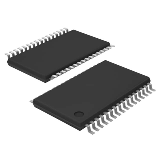
- Part No.:
- UJA1065TW/5V0/512
- Manufacturer:
- NXP Semiconductors
- Category:
- Specialized
- Package:
- 32-TSSOP (0.240", 6.10mm Width) Exposed Pad
- Datasheet:
-
 UJA1065TW/5V0/512.pdf
- Description:
- IC INTFACE SPECIALIZED 32HTSSOP
- Quantity:
- Payment:

- Shipping:

Inventory:1,349
Please send an inquiry. Send us your inquiry, and we will respond immediately.
Product details
Overview
UJA1065TW/5V0/512 from NXP Semiconductors is a fail-safe System Basis Chip (SBC) integrating high-speed CAN and LIN transceivers, dual voltage regulators (5.0 V for MCU and 5 V for CAN), an enhanced window watchdog with on-chip oscillator, SPI interface, and limp-home output. It serves as the central power, communication, and safety supervisor in automotive ECUs operating in 14 V or 42 V architectures.
For engineers reviewing the UJA1065TW/5V0/512 datasheet, UJA1065TW/5V0/512 pinout, UJA1065TW/5V0/512 application, or UJA1065TW/5V0/512 equivalent, key selection criteria include ISO 11898-2/ISO 11898-5 CAN compliance, LIN 2.0/SJ2602 support, fail-safe mode behavior, 32-pin HTSSOP package thermal performance, and 5.0 V microcontroller regulator output specification.
Technical Context
The UJA1065TW/5V0/512 implements a state-machine-based fail-safe system controller clocked by an on-chip oscillator, managing six distinct operating modes (Start-up, Restart, Normal, Standby, Sleep, Flash) with deterministic transitions triggered by reset events, watchdog timeouts, bus activity, or local wake-up. Its SPI interface uses fail-safe coded 16-bit messaging for register access and status reporting.
It integrates two independent transceivers: a high-speed CAN transceiver with SPLIT pin for recessive bus stabilization and partial networking support, and a LIN transceiver compliant with LIN 2.0 and SAE J2602, both featuring ±60 V short-circuit protection and bus-float capability when unpowered. The device supports remote flash programming via CAN and provides 23 bits of access-protected RAM for diagnostic logging.
Key Specifications
| Parameter | Value and Actual Design Meaning |
|---|---|
| CAN Standard | ISO 11898-2 and ISO 11898-5 compliant; ensures interoperability with TJA1041/TJA1041A and robust EMC in automotive networks. |
| LIN Standard | LIN 2.0 and SAE J2602 compliant; backward compatible with LIN 1.3 and TJA1020 for legacy sub-bus integration. |
| MCU Supply | 5.0 V regulated output (V1); fixed version per UJA1065TW/5V0 designation; powers external microcontroller with low dropout and undervoltage monitoring. |
| CAN Supply | 5 V dedicated regulator (V2); isolated from MCU supply and guarded by CAN-bus failure management to improve EMC. |
| Watchdog Type | Programmable fail-safe coded window and time-out watchdog; clocked by on-chip oscillator; prevents software deadlock with strict timing enforcement. |
| Package | HTSSOP32 (SOT549-1); 6.1 mm × 11 mm body, 0.65 mm pitch, exposed die pad for thermal dissipation and EMC optimization. |
| ESD Protection | ±8 kV HBM and ±4 kV IEC 61000-4-2 on off-board pins; meets automotive EMC requirements for harsh environments. |
| Bus Fault Tolerance | ±60 V short-circuit proof on CAN/LIN bus pins; battery and bus pins protected per ISO 7637-3 transients. |
Pinout & Package
UJA1065TW/5V0/512 is housed in a 32-pin HTSSOP package (SOT549-1) with 6.1 mm × 11 mm footprint, 0.65 mm lead pitch, and an exposed die pad for enhanced thermal conduction and EMC performance. The pad may be left floating or connected to GND.
| Pin/Terminal | Circuit Role | Design Meaning |
|---|---|---|
| V1 | Microcontroller supply output | 5.0 V regulated output; powers MCU core; monitored for undervoltage detection and fail-safe response. |
| V2 | CAN transceiver supply output | 5 V dedicated regulator output; independent of V1; improves CAN bus EMC and fault isolation. |
| RSTN | Reset output | Active-low open-drain reset signal to MCU; detects clamping conditions and initiates controlled start-up sequences. |
| INTN | Interrupt output | Active-low open-drain interrupt to MCU; wire-AND capable; signals faults including bus errors, overtemperature, and regulator failures. |
| INH/LIMP | Inhibit/limp-home output | BAT14-related push-pull output; floats by default; drives warning lights or failsafe hardware when system enters Fail-safe mode. |
| SCK/SDI/SDO/SCS | SPI interface | Full-duplex SPI bus (clock, input, output, chip select); uses fail-safe coded protocol for reliable register access and status reporting. |
| TXDC/RXDC | CAN data interface | CMOS-level inputs/outputs connecting to MCU's CAN controller; enable bidirectional high-speed CAN communication. |
| CANH/CANL | CAN bus interface | Differential bus lines compliant with ISO 11898-2; support dominant/recessive states and partial networking wake-up. |
| TXDL/RXDL | LIN data interface | CMOS-level LIN transmit/receive signals; interface directly with MCU's LIN controller or UART peripheral. |
| LIN/RTLIN | LIN bus interface | LIN bus line and internal termination resistor connection; enables single-wire LIN communication with built-in biasing. |
| WAKE | Local wake-up input | BAT42-related input; supports continuous or cyclic sampling to trigger wake-up from Standby/Sleep modes without bus traffic. |
| BAT14/BAT42 | Power supply inputs | Separate 14 V and 42 V battery inputs; allows operation in dual-voltage architectures; BAT42 connects to BAT14 in 14 V-only systems. |
| SYSINH | System inhibit output | BAT42-related output; controls external DC-DC converters or power domains during mode transitions. |
| V3 | Unregulated 42 V output | BAT42-derived output; configurable as continuous, OFF, or cyclic mode synchronized with WAKE for external load control. |
| SENSE | Battery interrupt input | Fast battery chatter detector input; enables rapid response to battery connection/disconnection events. |
Key Features
| Feature | Design Value |
|---|---|
| Fail-safe state machine | Hardware-enforced six-mode operation (Start-up, Restart, Normal, Standby, Sleep, Flash) with deterministic transitions and reset-source reporting for robust ECU boot and recovery. |
| Fail-safe SPI interface | 16-bit coded SPI protocol prevents misconfiguration; enables single-message status reporting (23-bit protected RAM, fault flags, mode info) without frame assembly. |
| Partial networking support | CAN transceiver supports global wake-up without waking sleeping nodes; reduces system-wide current consumption during selective communication. |
| Limp-home activation | INH/LIMP output asserts in Fail-safe mode to drive external warning lights or safety-critical hardware without MCU intervention. |
| Cyclic wake-up capability | Watchdog and WAKE pin support periodic wake-up from Standby/Sleep modes; enables ultra-low-power monitoring while preserving RAM content. |
| Integrated diagnostics | Detects and reports 12+ fault types including oscillator failure, bus shorts/opens, TXD/RXD clamping, reset line faults, SPI errors, overtemperature, and ground shift. |
Applications
| Body Control Module (BCM) | Engine Control Unit (ECU) |
|---|---|
Use Scenario: Centralized vehicle subsystem coordination including door locks, lighting, and climate control via CAN backbone and LIN sub-nodes. IC Role / Device Role / Timing Role: UJA1065TW/5V0/512 acts as primary power supervisor, CAN/LIN gateway, and fail-safe monitor-ensuring defined start-up, safe shutdown, and diagnostic reporting across distributed sensors and actuators. Use Value: Enables deterministic boot sequencing, remote flash updates over CAN, and limp-home activation of hazard lights during critical faults-meeting ASIL-B functional safety requirements. | Use Scenario: Real-time engine management requiring high-integrity communication between MCU, sensors (MAP, crankshaft), and actuators (injectors, ignition) under extreme temperature and EMI conditions. IC Role / Device Role / Timing Role: UJA1065TW/5V0/512 supplies regulated 5.0 V to MCU, isolates CAN transceiver power, monitors bus integrity, and enforces watchdog supervision to prevent runaway code execution. Use Value: Provides ±60 V bus fault tolerance, ISO 7637-3 transient protection, and detailed fault logging-reducing field failure root-cause analysis time by enabling post-event diagnostic retrieval via SPI. |
| Transmission Control Module (TCM) | Advanced Driver Assistance Systems (ADAS) Sensor Hub |
Use Scenario: Gearbox control unit interfacing with torque converter, solenoids, and gear position sensors using CAN for main network and LIN for low-cost sensor clusters. IC Role / Device Role / Timing Role: UJA1065TW/5V0/512 delivers stable 5.0 V MCU supply, manages CAN/LIN physical layers, and executes fail-safe transitions (e.g., entering Limp-home upon CAN bus failure). Use Value: Guarantees safe degradation paths (e.g., forced neutral gear engagement) via INH/LIMP output and preserves critical calibration data in protected RAM during brownout events. | Use Scenario: Aggregation and preprocessing of radar, camera, and ultrasonic sensor data before forwarding to central ADAS domain controller via high-speed CAN FD backbone. IC Role / Device Role / Timing Role: UJA1065TW/5V0/512 serves as power and communication foundation for edge sensor nodes-providing low-quiescent-current Sleep mode, cyclic wake-up for sensor polling, and robust LIN connectivity to passive sensors. Use Value: Achieves <100 µA sleep current with wake-on-LIN/CAN activity, enabling always-on sensor readiness while meeting OEM battery drain targets for parked vehicle scenarios. |
Equivalent & Alternatives
The following parts are listed as comparable options for similar fail-safe SBC applications.
| Alternative Part | Technical Difference | Application Difference | Selection Advice |
|---|---|---|---|
| UJA1075TW/5V0/512 | Successor device with extended CAN FD support, higher V3 drive capability (1.5 A vs. 0.5 A), and updated watchdog configuration registers. | Required for new designs targeting CAN FD communication or higher-current external loads; not drop-in due to register map changes and pinout revision. | Select UJA1075TW/5V0/512 for CAN FD-enabled platforms or where >0.5 A V3 drive is needed; retain UJA1065TW/5V0/512 for legacy 11-bit CAN and cost-sensitive 14 V systems. |
| TJA1021T/CM | Standalone LIN transceiver only; lacks CAN, regulators, watchdog, SPI, and fail-safe logic-requires external components to replicate UJA1065TW/5V0/512 functionality. | Suitable only for LIN-only nodes without safety-critical supervision; cannot replace UJA1065TW/5V0/512 in integrated ECU roles. | Choose TJA1021T/CM only for simple LIN slave nodes; UJA1065TW/5V0/512 remains necessary where integrated power, CAN, and fail-safe supervision are required. |
Compared with UJA1075TW/5V0/512, the UJA1065TW/5V0/512 offers proven reliability in mature 11-bit CAN architectures but lacks CAN FD and higher V3 drive; versus TJA1021T/CM, it delivers full SBC integration-eliminating board space, BOM count, and qualification effort for multi-function ECUs.
Availability
UJA1065TW/5V0/512 is available at Aetrix Electronics and suitable for automotive Body Control Modules, Engine Control Units, Transmission Control Modules, and ADAS sensor hubs requiring stable component supply, long-term lifecycle support, and AEC-Q100 qualified reliability.
Supply support for UJA1065TW/5V0/512 includes scheduled delivery planning, volume procurement assistance, BOM continuity management, traceable sourcing, and lifecycle availability coordination for OEM customers, industrial embedded developers, connected-device designers, and electronics production programs.
Manufacturer
NXP Semiconductors is a global semiconductor leader specializing in secure connectivity solutions for automotive, industrial, and IoT applications, with deep expertise in automotive-grade mixed-signal ICs.
The UJA1065TW/5V0/512 belongs to NXP's System Basis Chip product line, designed specifically to consolidate power, communication, and safety functions into a single AEC-Q100 qualified device for next-generation automotive ECUs.
FAQ
What is the primary function of the UJA1065TW/5V0/512 in an automotive ECU?
The UJA1065TW/5V0/512 serves as a fail-safe System Basis Chip that integrates high-speed CAN and LIN transceivers, dual voltage regulators (5.0 V for MCU and 5 V for CAN), an enhanced watchdog, SPI interface, and limp-home output. It replaces discrete components to provide centralized power management, communication interfacing, and autonomous fault detection-ensuring safe and predictable ECU behavior across all operating modes. Its design enables deterministic start-up, robust bus communication, and graceful degradation during faults.
Does the UJA1065TW/5V0/512 support both 14 V and 42 V automotive battery architectures?
Yes, the UJA1065TW/5V0/512 is explicitly designed for dual-voltage operation. It accepts separate BAT14 (14 V) and BAT42 (42 V) inputs, allowing use in conventional 14 V systems (with BAT42 tied to BAT14) or advanced 42 V architectures. Its V3 output is BAT42-related and configurable in continuous, OFF, or cyclic mode-supporting external 42 V loads like relays or wake-up switches. This dual-supply capability makes UJA1065TW/5V0/512 suitable for scalable ECU designs across vehicle platforms.
How does the fail-safe watchdog in the UJA1065TW/5V0/512 differ from standard watchdog timers?
The UJA1065TW/5V0/512 features a programmable fail-safe coded watchdog clocked by an on-chip oscillator, supporting Start-up, Window, Time-out, and OFF modes. Unlike generic watchdogs, it uses redundant bit coding for all SPI accesses-only ten valid period codes and six valid mode codes are accepted. Illegal triggers cause immediate reset. In Normal mode, it enforces strict timing windows (50–100% of period); early or late servicing forces entry into Start-up mode. This architecture prevents software lockup and ensures deterministic recovery-core to UJA1065TW/5V0/512's role in ASIL-B–capable systems.
What are the key differences between the UJA1065TW/5V0/512 and the UJA1075TW/5V0/512?
The UJA1075TW/5V0/512 is the functional successor to the UJA1065TW/5V0/512, adding CAN FD support, increasing V3 output drive capability to 1.5 A (vs. 0.5 A), and updating register mapping and watchdog configuration logic. While both share identical pinout and core SBC functionality, UJA1075TW/5V0/512 is not pin-compatible due to revised pin assignments and requires firmware adaptation. UJA1065TW/5V0/512 remains optimal for cost-sensitive 11-bit CAN applications where CAN FD is unnecessary and legacy qualification is required.
Can the UJA1065TW/5V0/512 perform remote firmware updates over the CAN bus?
Yes, the UJA1065TW/5V0/512 supports remote flash programming via the CAN bus. Its fail-safe architecture enables secure entry into Flash mode through a three-step SPI handshake (111→001→111 sequence), after which the microcontroller can execute firmware updates. During Flash mode, the watchdog operates in time-out mode with strict code validation (only 111 allowed for servicing), and improper access triggers immediate reset. This capability allows OEMs to deploy over-the-air (OTA) updates while maintaining functional safety-making UJA1065TW/5V0/512 suitable for modern connected vehicle ECUs.
UJA1065TW/5V0/512 Specifications
- Product attributes
- Attribute value
- Manufacturer:
- NXP Semiconductors
- Series:
- -
- Package/Case:
- 32-TSSOP (0.240", 6.10mm Width) Exposed Pad
- Packaging:
- Tube
- Product Status:
- Obsolete
- Applications:
- Networking
- Interface:
- SPI Serial
- Voltage - Supply:
- 5.5V ~ 52V
- Supplier Device Package:
- 32-HTSSOP
- Grade:
- Automotive
- Qualification:
- -
- Mounting Type:
- Surface Mount
UJA1065TW/5V0/512 FAQ
1.How can I place an order for UJA1065TW/5V0/512 through Aetrix?
Please submit a Request for Quotation (RFQ) for UJA1065TW/5V0/512 on Aetrix. Our sales agent will provide a competitive quotation and guide you through the order confirmation once you accept the terms.
2.Are the price and stock information for UJA1065TW/5V0/512 reliable?
The price and inventory of UJA1065TW/5V0/512 are updated periodically and may fluctuate due to market conditions. Stock and pricing data are typically refreshed every 24 hours. Quotation validity for UJA1065TW/5V0/512 is usually 5 days.
3.What payment methods are accepted for UJA1065TW/5V0/512?
We accept Wire Transfer, PayPal, Credit Card, Western Union, MoneyGram, and Escrow for UJA1065TW/5V0/512 transactions.
Note: Certain payment methods may incur a processing fee.
4.How is shipping managed for UJA1065TW/5V0/512?
UJA1065TW/5V0/512 orders can be shipped via leading logistics carriers, including DHL, UPS, FedEx, TNT, or Registered Mail.
Once your UJA1065TW/5V0/512 order is processed, you will receive an email with the shipment details and tracking number.
Note: Tracking information may take up to 24 hours to appear. Express delivery typically takes 3–5 business days.
5.How can I obtain technical support or documentation for UJA1065TW/5V0/512?
For technical support, including UJA1065TW/5V0/512 datasheets, pinout diagrams, or application guidance, please contact our engineering support team. They can provide detailed documentation and assistance for your UJA1065TW/5V0/512 requirements.
6.How does Aetrix verify that UJA1065TW/5V0/512 is sourced from the original manufacturer or authorized distributors?
All UJA1065TW/5V0/512 products on Aetrix are procured from qualified distributors and authorized channels. Our dedicated quality assurance team conducts strict verification, including traceability checks and, if necessary, third-party testing. This ensures that UJA1065TW/5V0/512 meets industry standards.
7.What is the process for return or replacement of UJA1065TW/5V0/512?
All UJA1065TW/5V0/512 units undergo pre-shipment inspection (PSI). If there is an issue with UJA1065TW/5V0/512, returns or replacements are accepted under the following conditions:
1.Quantity discrepancies, incorrect items, or visible external defects (such as breakage or corrosion), acknowledged by Aetrix.
2.The issue is reported within 90 days of delivery.
3.The UJA1065TW/5V0/512 part is unused and in its original packaging.
Return procedure for UJA1065TW/5V0/512:
1.Submit a request within 90 days.
2.Obtain a Return Material Authorization (RMA) from Aetrix.
UJA1065TW/5V0/512 Tags

-
NVT4857UKAZ
NXP Semiconductors

-
TCA8418RTWR
Texas Instruments

-
PCA9546APWR
Texas Instruments

-
MD0100N8-G
Microchip Technology

-
PCA9548APW,118
NXP Semiconductors

-
PCA9540BDP,118
NXP Semiconductors

-
PCA9548APWR
Texas Instruments

-
PCA9546APW,118
NXP Semiconductors

-
PTN3360DBS,518
NXP Semiconductors

-
PCA9546ABS,118
NXP Semiconductors

-
PCA9518PWR
Texas Instruments

-
PCA9545APW,118
NXP Semiconductors
Tech Hub

A practical engineering guide to 3.3V and 5V logic compatibility, input thresholds, resistor dividers, translator ICs, MOSFET level shifting, I2C pull-ups, timing limits and power-sequencing risks.

The 74HC595 uses push-pull logic outputs, while the TPIC6B595 uses 50 V open-drain DMOS sinks for higher-power loads. This guide compares timing, current limits, 3.3 V interfacing, load wiring, thermal…

The 74HC595 converts serial data into eight stable parallel outputs. This guide covers pin functions, shift and storage timing, OE and MR behavior, drive-current limits, cascading, voltage compatibilit…

A technical comparison of level-sensitive latches and edge-triggered flip-flops, covering timing windows, setup and hold limits, master–slave operation, time borrowing, race-through, HDL inference and…

A D latch stores one bit while Enable controls when data can pass. This reference covers gate-level operation, truth tables, transparency, setup and hold timing, LE versus OE, common ICs and practical …

An SR latch stores one bit through cross-coupled feedback. This engineering reference covers NOR and NAND implementations, truth tables, forbidden-state recovery, gated operation, switch debouncing, fa…

Latch circuits retain one bit through feedback. This technical reference covers SR and D latches, truth tables, transparency, timing limits, latch-versus-flip-flop behavior, applications and common log…

An engineering guide to LED driver operation, constant-current and constant-voltage outputs, linear and switching topologies, dimming, IC selection, calculations, replacement compatibility, and fault c…

Operational amplifier guide covering op amp basics, feedback, ideal vs real op amps, common configurations, buffer circuits, offset, bias current, gain-bandwidth, slew rate, rail-to-rail limits and sel…

Jumper cables guide covering safe connection order, red and black clamp placement, final ground connection, cable gauge, length, clamp quality, copper vs CCA cables, jump starter comparison and battery…


