
 My Inquiry
 My Account


NXP Semiconductors UJA1079TW/3V3/WD,1
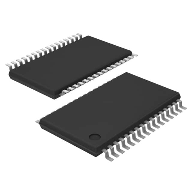
- Part No.:
- UJA1079TW/3V3/WD,1
- Manufacturer:
- NXP Semiconductors
- Category:
- Specialized
- Package:
- 32-TSSOP (0.240", 6.10mm Width) Exposed Pad
- Datasheet:
-
 UJA1079TW/3V3/WD,1.pdf
- Description:
- IC INTFACE SPECIALIZED 32HTSSOP
- Quantity:
- Payment:

- Shipping:

Inventory:2,846
Please send an inquiry. Send us your inquiry, and we will respond immediately.
Product details
Overview
UJA1079TW/3V3/WD from NXP Semiconductors is a LIN 2.1–compliant System Basis Chip (SBC) integrating a 3.3 V/250 mA voltage regulator, advanced window/timeout watchdog with on-chip oscillator, LIN transceiver with integrated termination diode, SPI interface, dual local wake-up inputs, and limp-home output - designed for automotive ECU power management and communication control in body electronics and sensor modules.
For engineers reviewing the UJA1079TW/3V3/WD datasheet, UJA1079TW/3V3/WD pinout, UJA1079TW/3V3/WD application, or UJA1079TW/3V3/WD equivalent, key selection considerations include its HTSSOP32 package thermal performance, ±58 V short-circuit protected LIN bus pin, 3.3 V regulator accuracy (±2 % for master, ±3 % for slave), programmable wake-up sampling (16 ms/64 ms), and watchdog behavior under reset conditions.
Technical Context
The UJA1079TW/3V3/WD implements a state-machine-based system controller managing Off/Standby/Normal/Sleep/Overtemp modes with deterministic transitions triggered by VBAT thresholds, wake events, or temperature. Its LIN transceiver supports low-slope mode (10.4 kbit/s) for EMC optimization and includes DLIN-connected internal termination diode.
Power management integrates V1 regulation with external PNP transistor support (VEXCTRL/VEXCC pins), selectable current thresholds (50/85 mA activation), and undervoltage detection at 90 % or 70 % of nominal output. The watchdog operates independently via on-chip oscillator and supports Window mode (with ttrig(wd)1/ttrig(wd)2 timing windows) and Timeout mode with cyclic interrupt capability.
Key Specifications
| Parameter | Value and Actual Design Meaning |
|---|---|
| LIN Compliance | LIN 2.1, SAE J2602, backward-compatible with LIN 2.0 and LIN 1.3 - ensures interoperability in legacy and new automotive networks. |
| Voltage Regulator | 3.3 V ±2 % (master), ±3 % (slave); 250 mA max; supports external PNP for thermal distribution - powers MCU and peripherals without external LDO. |
| Watchdog Modes | Window, Timeout, Off; programmable period (8–4096 ms); independent on-chip oscillator clock - enables fail-safe timing supervision across all ECU states. |
| SPI Interface | 16-bit full-duplex; register-mapped read/write access; SCSN-active-low, SCK-falling-edge sample - enables real-time configuration and status reporting to MCU. |
| Thermal Protection | Overtemperature shutdown with hysteresis; LIMP output activated on OTP entry - triggers hardware limp-home response before thermal damage occurs. |
| ESD & Transient Robustness | ±8 kV HBM, ±6 kV IEC 61000-4-2 on LIN/WAKE pins; ±58 V short-circuit proof LIN; ISO 7637-3 transient protection - meets automotive EMC requirements without external clamping. |
| Wake-Up Capability | Two dedicated WAKE1/WAKE2 inputs with configurable sampling (16 ms/64 ms), bias control (WBIAS), and interrupt generation - enables ultra-low-power standby with reliable event detection. |
Pinout & Package
Package: HTSSOP32 (SOT549-1), 6.1 mm × 11 mm, 0.65 mm pitch, exposed die pad for PCB thermal conduction.
| Pin/Terminal | Circuit Role | Design Meaning |
|---|---|---|
| V1 (Pin 4) | Regulated output | 3.3 V supply for MCU and peripherals; undervoltage warning/reset at 90 % or 70 % threshold. |
| RXDL (Pin 5) | LIN receive data | Logic-level output reflecting LIN bus state; used for wake-up flag and diagnostics. |
| RSTN (Pin 6) | Bidirectional reset | Drives LOW on internal reset events; accepts external LOW for forced reset; pulse width configurable via pull-up. |
| INTN (Pin 7) | Interrupt output | Open-drain signal indicating V1 UV, LIN/local wake, cyclic, or power-on events - enables prioritized MCU servicing. |
| EN (Pin 8) | Global enable output | Fail-safe control signal to enable/disable safety-critical downstream circuitry in Normal mode. |
| WAKE1 (Pin 18) | Local wake input | Dedicated wake source with configurable sampling and interrupt edge detection - reduces standby current vs. polling. |
| WAKE2 (Pin 19) | Local wake input | Second independent wake channel supporting rising/falling/both-edge triggering - enables multi-sensor wake architecture. |
| LIMP (Pin 17) | Limp-home output | Active-LOW fail-safe signal to activate degraded-mode hardware during Overtemp or critical fault - prevents unsafe operation. |
| WDOFF (Pin 16) | Watchdog disable | Hardware override: HIGH disables watchdog regardless of register settings - supports debug and safe boot sequences. |
| VEXCTRL (Pin 31) | PNP base control | Drives external PNP transistor base to extend V1 current capability and distribute heat across PCB. |
| VEXCC (Pin 29) | PNP collector sense | Monitors external PNP collector current to coordinate V1 load sharing and prevent overcurrent. |
| DLIN (Pin 26) | LIN termination diode | Internal diode connection point for LIN bus termination - eliminates discrete diode and saves board space. |
Key Features
| Feature | Design Value |
|---|---|
| Advanced Low-Power Concept | Standby current < 100 µA with full wake-up capability; Sleep mode cuts V1 to reduce system leakage - extends battery life in always-on ECUs. |
| Safe System Start-Up | Deterministic power-on reset sequence with configurable pulse width and VBAT threshold detection - ensures MCU boots only when V1 is stable. |
| Detailed Status Reporting | Register-mapped diagnostics including V1 status, wake-source flags, interrupt pending bits, and watchdog state - enables precise fault isolation without external logic. |
| LIN Bus EMC Optimization | Low-slope mode (10.4 kbit/s) and integrated DLIN termination diode - reduces radiated emissions and simplifies layout vs. discrete solutions. |
| Fail-Safe Hardware Outputs | Dedicated EN (global enable) and LIMP (limp-home) pins with guaranteed behavior during faults - replaces discrete safety monitoring circuits. |
Applications
| Body Control Module (BCM) | Seat Position Control |
|---|---|
Use Scenario: Centralized control of door locks, windows, mirrors, and interior lighting in passenger vehicles. IC Role / Device Role / Timing Role: UJA1079TW/3V3/WD serves as primary power manager and LIN interface hub, regulating MCU supply, supervising startup, and relaying commands between LIN master and slave nodes. Use Value: Eliminates discrete regulators, watchdogs, and LIN transceivers while providing certified automotive-grade robustness and thermal management in compact HTSSOP32 footprint. | Use Scenario: Motorized adjustment of driver/passenger seat position using LIN-connected potentiometers and actuators. IC Role / Device Role / Timing Role: UJA1079TW/3V3/WD supplies 3.3 V to seat MCU, detects local switch wake events (WAKE1/WAKE2), and reports faults via SPI to main BCM over LIN. Use Value: Enables ultra-low-power sleep (< 100 µA) with reliable wake-up from mechanical switches and failsafe limp-home activation if motor stalls or overheats. |
| Roof Module (Sunroof/Climate) | Trunk/Liftgate Actuation |
Use Scenario: Integrated control of sunroof glass/motor and HVAC blend doors via LIN sub-network. IC Role / Device Role / Timing Role: UJA1079TW/3V3/WD provides regulated 3.3 V power, monitors LIN bus activity for remote wake, and triggers LIMP output if temperature exceeds safe limit during extended actuation. Use Value: Delivers ±58 V short-circuit protection on LIN pin and ±8 kV ESD immunity - withstands harsh roof module environments with minimal external protection. | Use Scenario: Power liftgate systems requiring controlled motor sequencing, obstacle detection, and battery-conscious operation. IC Role / Device Role / Timing Role: UJA1079TW/3V3/WD manages MCU power, detects trunk open/close switch events via WAKE1/WAKE2, and asserts LIMP to halt motor drive on overtemperature or V1 undervoltage. Use Value: Integrates watchdog supervision with programmable window timing - prevents runaway motor operation due to software hang while maintaining ASIL-B–aligned safety behavior. |
Equivalent & Alternatives
The following parts are listed as comparable options for similar LIN SBC applications.
| Alternative Part | Technical Difference | Application Difference | Selection Advice |
|---|---|---|---|
| UJA1076TW/3V3/WD | Same HTSSOP32 package and 3.3 V regulator, but lacks LIMP output and has reduced SPI register set - no limp-home fail-safe capability. | Targeted at cost-sensitive LIN slaves where degraded-mode hardware activation is not required. | Select UJA1076TW/3V3/WD only if limp-home functionality is omitted from system architecture and diagnostic depth is reduced. |
| TLE9471-2ES | Infineon LIN SBC with 3.3 V/250 mA regulator, integrated CAN transceiver, and higher integration (e.g., high-side drivers), but larger TQFP48 package and different pinout. | Used in mixed LIN/CAN gateways or modules requiring additional drive capability beyond basic SBC functions. | Choose TLE9471-2ES when CAN coexistence or embedded high-side switching is needed - not a drop-in replacement due to package and interface differences. |
Compared with UJA1076TW/3V3/WD, the UJA1079TW/3V3/WD adds essential limp-home fail-safe output and richer SPI diagnostics; versus TLE9471-2ES, it offers smaller footprint and LIN-optimized features but lacks CAN integration - making UJA1079TW/3V3/WD optimal for pure LIN body electronics with strict space and safety requirements.
Availability
UJA1079TW/3V3/WD is available at Aetrix Electronics and suitable for automotive body electronics, seat control modules, roof modules, and liftgate actuation systems requiring stable component supply, long-term lifecycle assurance, and AEC-Q100–aligned reliability.
Supply support for UJA1079TW/3V3/WD includes scheduled delivery planning, volume procurement assistance, BOM continuity management, traceable sourcing, and lifecycle availability coordination for OEM customers, industrial embedded developers, connected-device designers, and electronics production programs.
Manufacturer
NXP Semiconductors is a global semiconductor leader specializing in secure connectivity solutions for automotive, industrial, and IoT applications, with deep expertise in automotive-grade analog and mixed-signal ICs.
The UJA1079TW/3V3/WD belongs to NXP's System Basis Chip product line, engineered specifically for automotive LIN networked ECUs to consolidate power, communication, and safety functions into a single robust, thermally optimized device.
FAQ
What LIN protocol versions does the UJA1079TW/3V3/WD support?
The UJA1079TW/3V3/WD supports LIN 2.1 and SAE J2602 as primary standards, with full backward compatibility to LIN 2.0 and LIN 1.3. This ensures seamless integration into legacy vehicle architectures while enabling compliance with current automotive LIN specifications. All protocol handling is implemented in hardware within the transceiver block of the UJA1079TW/3V3/WD.
How does the UJA1079TW/3V3/WD manage thermal dissipation in automotive environments?
The UJA1079TW/3V3/WD uses an HTSSOP32 package with an exposed die pad that conducts heat directly into the PCB copper, significantly lowering junction-to-board thermal resistance. When paired with an external PNP transistor via VEXCTRL/VEXCC pins, it distributes regulator power dissipation across the board - enabling sustained 250 mA output even at 125 °C ambient, as validated in NXP's thermal characterization of the UJA1079TW/3V3/WD.
Can the UJA1079TW/3V3/WD operate during automotive cranking conditions?
Yes, the UJA1079TW/3V3/WD maintains stable 3.3 V regulation down to VBAT = 4.5 V, meeting ISO 7637-3 pulse 4/4b and ISO 16750-2 cranking requirements. Its V1 regulator remains active and delivers full 250 mA during cranking, and the watchdog continues operating from its independent VBAT-supplied oscillator - ensuring continuous supervision of the MCU throughout engine start cycles.
What is the function of the WDOFF pin on the UJA1079TW/3V3/WD?
The WDOFF pin on the UJA1079TW/3V3/WD provides hardware-level watchdog disable: pulling it HIGH forces the watchdog into Off mode regardless of register settings or operating state. This enables safe debug sessions, bootloader execution, or controlled system initialization sequences. When WDOFF is LOW, watchdog behavior is governed by the WMC bit and current SBC mode - a key safety feature unique to the UJA1079TW/3V3/WD design.
Does the UJA1079TW/3V3/WD support both rising- and falling-edge wake-up detection?
Yes, the UJA1079TW/3V3/WD supports configurable edge detection on both WAKE1 and WAKE2 pins via the Int_Control register (bits WIC1/WIC2). Each wake input can be set to trigger interrupts on rising edge, falling edge, or both edges - allowing flexible interfacing with mechanical switches, Hall sensors, or other wake sources without external signal conditioning. This capability is fully documented in the UJA1079TW/3V3/WD datasheet Section 6.2.5.
UJA1079TW/3V3/WD,1 Specifications
- Product attributes
- Attribute value
- Manufacturer:
- NXP Semiconductors
- Series:
- -
- Package/Case:
- 32-TSSOP (0.240", 6.10mm Width) Exposed Pad
- Packaging:
- Tape & Reel (TR)
- Product Status:
- Obsolete
- Applications:
- -
- Interface:
- SPI Serial
- Voltage - Supply:
- 4.5V ~ 28V
- Supplier Device Package:
- 32-HTSSOP
- Grade:
- Automotive
- Qualification:
- -
- Mounting Type:
- Surface Mount
UJA1079TW/3V3/WD,1 FAQ
1.How can I place an order for UJA1079TW/3V3/WD,1 through Aetrix?
Please submit a Request for Quotation (RFQ) for UJA1079TW/3V3/WD,1 on Aetrix. Our sales agent will provide a competitive quotation and guide you through the order confirmation once you accept the terms.
2.Are the price and stock information for UJA1079TW/3V3/WD,1 reliable?
The price and inventory of UJA1079TW/3V3/WD,1 are updated periodically and may fluctuate due to market conditions. Stock and pricing data are typically refreshed every 24 hours. Quotation validity for UJA1079TW/3V3/WD,1 is usually 5 days.
3.What payment methods are accepted for UJA1079TW/3V3/WD,1?
We accept Wire Transfer, PayPal, Credit Card, Western Union, MoneyGram, and Escrow for UJA1079TW/3V3/WD,1 transactions.
Note: Certain payment methods may incur a processing fee.
4.How is shipping managed for UJA1079TW/3V3/WD,1?
UJA1079TW/3V3/WD,1 orders can be shipped via leading logistics carriers, including DHL, UPS, FedEx, TNT, or Registered Mail.
Once your UJA1079TW/3V3/WD,1 order is processed, you will receive an email with the shipment details and tracking number.
Note: Tracking information may take up to 24 hours to appear. Express delivery typically takes 3–5 business days.
5.How can I obtain technical support or documentation for UJA1079TW/3V3/WD,1?
For technical support, including UJA1079TW/3V3/WD,1 datasheets, pinout diagrams, or application guidance, please contact our engineering support team. They can provide detailed documentation and assistance for your UJA1079TW/3V3/WD,1 requirements.
6.How does Aetrix verify that UJA1079TW/3V3/WD,1 is sourced from the original manufacturer or authorized distributors?
All UJA1079TW/3V3/WD,1 products on Aetrix are procured from qualified distributors and authorized channels. Our dedicated quality assurance team conducts strict verification, including traceability checks and, if necessary, third-party testing. This ensures that UJA1079TW/3V3/WD,1 meets industry standards.
7.What is the process for return or replacement of UJA1079TW/3V3/WD,1?
All UJA1079TW/3V3/WD,1 units undergo pre-shipment inspection (PSI). If there is an issue with UJA1079TW/3V3/WD,1, returns or replacements are accepted under the following conditions:
1.Quantity discrepancies, incorrect items, or visible external defects (such as breakage or corrosion), acknowledged by Aetrix.
2.The issue is reported within 90 days of delivery.
3.The UJA1079TW/3V3/WD,1 part is unused and in its original packaging.
Return procedure for UJA1079TW/3V3/WD,1:
1.Submit a request within 90 days.
2.Obtain a Return Material Authorization (RMA) from Aetrix.
UJA1079TW/3V3/WD,1 Tags

-
NVT4857UKAZ
NXP Semiconductors

-
TCA8418RTWR
Texas Instruments

-
PCA9546APWR
Texas Instruments

-
MD0100N8-G
Microchip Technology

-
PCA9548APW,118
NXP Semiconductors

-
PCA9540BDP,118
NXP Semiconductors

-
PCA9548APWR
Texas Instruments

-
PCA9546APW,118
NXP Semiconductors

-
PTN3360DBS,518
NXP Semiconductors

-
PCA9546ABS,118
NXP Semiconductors

-
PCA9518PWR
Texas Instruments

-
PCA9545APW,118
NXP Semiconductors
Tech Hub

A practical engineering guide to 3.3V and 5V logic compatibility, input thresholds, resistor dividers, translator ICs, MOSFET level shifting, I2C pull-ups, timing limits and power-sequencing risks.

The 74HC595 uses push-pull logic outputs, while the TPIC6B595 uses 50 V open-drain DMOS sinks for higher-power loads. This guide compares timing, current limits, 3.3 V interfacing, load wiring, thermal…

The 74HC595 converts serial data into eight stable parallel outputs. This guide covers pin functions, shift and storage timing, OE and MR behavior, drive-current limits, cascading, voltage compatibilit…

A technical comparison of level-sensitive latches and edge-triggered flip-flops, covering timing windows, setup and hold limits, master–slave operation, time borrowing, race-through, HDL inference and…

A D latch stores one bit while Enable controls when data can pass. This reference covers gate-level operation, truth tables, transparency, setup and hold timing, LE versus OE, common ICs and practical …

An SR latch stores one bit through cross-coupled feedback. This engineering reference covers NOR and NAND implementations, truth tables, forbidden-state recovery, gated operation, switch debouncing, fa…

Latch circuits retain one bit through feedback. This technical reference covers SR and D latches, truth tables, transparency, timing limits, latch-versus-flip-flop behavior, applications and common log…

An engineering guide to LED driver operation, constant-current and constant-voltage outputs, linear and switching topologies, dimming, IC selection, calculations, replacement compatibility, and fault c…

Operational amplifier guide covering op amp basics, feedback, ideal vs real op amps, common configurations, buffer circuits, offset, bias current, gain-bandwidth, slew rate, rail-to-rail limits and sel…

Jumper cables guide covering safe connection order, red and black clamp placement, final ground connection, cable gauge, length, clamp quality, copper vs CCA cables, jump starter comparison and battery…


