
 My Inquiry
 My Account


NXP Semiconductors UJA1169LTK/XZ
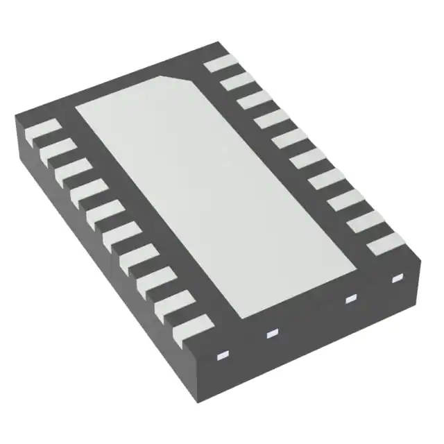
- Part No.:
- UJA1169LTK/XZ
- Manufacturer:
- NXP Semiconductors
- Category:
- Specialized
- Package:
- 20-VFDFN Exposed Pad
- Datasheet:
-
 UJA1169LTK/XZ.pdf
- Description:
- IC INTFACE SPECIALIZED 20HVSON
- Quantity:
- Payment:

- Shipping:

Inventory:1,454
Please send an inquiry. Send us your inquiry, and we will respond immediately.
Product details
Overview
UJA1169LTK/XZ from NXP Semiconductors is a mini high-speed CAN companion System Basis Chip (SBC) designed for automotive applications requiring dual-SBC architectures. It integrates an ISO 11898-2:201x/ISO 11898-6:2013-compliant HS-CAN transceiver, a scalable 5 V/250 mA regulator (V1), and SPI-controlled power management with Standby/Sleep modes, LIMP output, and watchdog functionality. It supports CAN FD-passive partial networking and operates with VIO input compatible with 3.3 V–5 V microcontrollers.
For engineers reviewing the UJA1169LTK/XZ datasheet, UJA1169LTK/XZ pinout, UJA1169LTK/XZ application, or UJA1169LTK/XZ equivalent, key selection considerations include its dedicated VIO interface for cross-domain compatibility, VEXT short-circuit protection to ±58 V and −18 V, autonomous bus biasing, CAN FD-passive wake-up suppression, and non-volatile configuration of V1 undervoltage thresholds and limp-home behavior.
Technical Context
The UJA1169LTK/XZ implements a dual-regulator architecture: V1 (5 V/250 mA) supplies external loads and the internal CAN transceiver, while VEXT (5 V/100 mA) provides protected off-board sensor power with short-circuit proofing to BAT, GND, and −18 V. Its CAN transceiver complies with ISO 11898-2:201x and ISO 11898-6:2013, enabling reliable CAN FD fast-phase communication up to 2 Mbit/s and selective wake-up frame detection.
Power management is governed by a state machine supporting Normal, Standby, Sleep, Reset, Forced Normal, Overtemp, and Off modes. Wake-up sources include CAN bus activity (standard or selective), local WAKE pin, and diagnostic events (overtemperature, watchdog failure); all trigger RXD LOW and are distinguishable via RSS bits in the Main status register (0x03). The integrated watchdog offers Window, Timeout, and Autonomous modes with programmable periods from 8 ms to 4 s.
Key Specifications
| Parameter | Value and Actual Design Meaning |
|---|---|
| CAN Compliance | ISO 11898-2:201x and ISO 11898-6:2013; enables CAN FD-passive partial networking and 2 Mbit/s fast-phase operation |
| V1 Regulator | 5 V ±2 %, 250 mA; remains operational down to 2 V battery input; includes selectable undervoltage detection thresholds (60–90 %) |
| VEXT Output | 5 V ±2 %, 100 mA; short-circuit proof to BAT, GND, and −18 V; user-controllable via SPI |
| Quiescent Current | <20 µA in Sleep mode; <50 µA in Standby mode; full wake-up capability retained |
| ESD Protection | ±6 kV IEC 61000-4-2 on BAT, WAKE, VEXT, and CAN pins; ±8 kV HBM on CAN pins |
| Thermal Protection | Overtemperature warning at Tth(warn)otp; automatic shutdown at Tth(act)otp; LIMP output triggered on overtemperature or watchdog failure |
| SPI Interface | 16-/24-/32-bit; supports configuration, diagnostics, and mode control; accessible in Normal, Standby, Forced Normal, and Reset modes |
Pinout & Package
Package: HVSON20 (3.5 mm × 5.5 mm × 0.85 mm), leadless, halogen-free, RoHS-compliant, with exposed die pad for enhanced thermal dissipation and grounding.
| Pin/Terminal | Circuit Role | Design Meaning |
|---|---|---|
| GND (Pins 1, 4, 16, 19) | Ground reference | Four dedicated ground terminals ensure low-impedance return paths for V1, VEXT, CAN, and digital logic; exposed die pad must be connected to PCB GND |
| TXD (Pin 2) | CAN transmit input | Accepts CMOS-level transmit data from MCU; drives internal CAN transceiver driver stage |
| SDI (Pin 3) | SPI data input | Serial data input for SPI configuration and control; level-shifted via VIO supply |
| V1 (Pin 5) | Main application supply output | 5 V/250 mA regulated output; powers external transceivers, sensors, or logic; remains active in Standby mode |
| VIO (Pin 6) | I/O level shifter supply | Accepts 3.3 V–5 V input to adapt digital interface to host MCU voltage domain; eliminates reverse supply current risk |
| VEXCC (Pin 7) | External PNP collector sense | Monitors current through external PNP transistor for thermal scaling of V1; enables adjustable current limiting |
| RXD (Pin 8) | CAN receive output / wake indicator | Reflects bus data stream in Normal mode; forced LOW on any enabled wake-up event (CAN, WAKE, diagnostic) |
| SDO (Pin 9) | SPI data output | Serial data output for readback of status registers and diagnostics; level-shifted via VIO |
| SCK (Pin 10) | SPI clock input | Drives synchronous SPI communication; timing defined per SPI specification (CPOL=0, CPHA=0) |
| LIMP (Pin 11) | Limp-home fault signal | Open-drain, active-LOW output; asserted on overtemperature or watchdog failure; configurable activation threshold |
| WAKE (Pin 12) | Local wake-up input | Active-LOW input for hardware-triggered wake-up; debounced internally; wake source identifiable via RSS bits |
| VEXT (Pin 13) | Off-board sensor supply | 5 V/100 mA protected output; short-circuit proof to BAT, GND, and −18 V; controlled via SPI register VEXTC/VEXTSUC |
| BAT (Pin 14) | Battery supply input | Input for automotive battery (4.5 V–40 V); protected against ISO 7637-3 transients and reverse polarity |
| VEXCTRL (Pin 15) | External PNP base control | Drives base of external PNP transistor to scale V1 current; enables thermal management without internal power loss |
| CANL (Pin 17) | CAN bus low line | Differential low-side connection to HS-CAN bus; floating when BAT = 0 V; ±58 V short-circuit rated |
| CANH (Pin 18) | CAN bus high line | Differential high-side connection to HS-CAN bus; floating when BAT = 0 V; ±58 V short-circuit rated |
| SCSN (Pin 20) | SPI chip select input | Active-LOW enable for SPI communication; synchronizes SDO/SDI transfers with SCK |
Key Features
| Feature | Design Value |
|---|---|
| CAN FD-passive partial networking | Enables Sleep/Standby mode during CAN FD traffic without bus errors; supports mixed CAN FD/classic CAN networks |
| VIO input for domain isolation | Eliminates reverse supply currents between primary and secondary SBCs by decoupling digital I/O from V1 domain |
| VEXT short-circuit protection | Withstands faults to BAT, GND, and negative voltages down to −18 V-critical for under-hood sensor interfaces |
| Non-volatile configuration storage | Persists V1 undervoltage thresholds, SLPC (Sleep disable), FNMC (Forced Normal), and limp-home activation settings across power cycles |
| Autonomous bus biasing | Maintains CAN bus termination at ~2.5 V during activity and biases to GND during silence (t > tto(silence)), reducing EMI and power |
Applications
| Body Control Module (BCM) | Advanced Driver Assistance Systems (ADAS) Sensor Hub |
|---|---|
Use Scenario: Centralized power and communication management for door modules, lighting, and seat controls in modern vehicle architectures. IC Role / Device Role / Timing Role: Companion SBC providing isolated 5 V power (V1/VEXT), HS-CAN interface, and fail-safe LIMP signaling to MCU in secondary domain. Use Value: Enables scalable addition of CAN nodes without redesigning primary SBC domain; VIO prevents reverse current flow during domain mismatch. | Use Scenario: Powering and interfacing radar, camera, and ultrasonic sensors in ADAS domain with strict functional safety requirements. IC Role / Device Role / Timing Role: Secondary SBC delivering protected 5 V sensor supply (VEXT), CAN FD-passive wake-up, and independent watchdog with ASIL-capable LIMP output. Use Value: Supports ASIL-B/C system partitioning via dedicated LIMP assertion on overtemperature or watchdog failure; VEXT short-circuit resilience ensures sensor uptime. |
| Electric Power Steering (EPS) Subsystem | Automotive Gateway Expansion Node |
Use Scenario: Adding redundant CAN connectivity and auxiliary power to EPS motor control units where space and thermal constraints limit integration. IC Role / Device Role / Timing Role: Mini SBC supplying 5 V to external transceivers and monitoring bus health via autonomous biasing and wake-source recognition. Use Value: Reduces BOM count by eliminating discrete regulators and level shifters; ultra-low Sleep current (<20 µA) extends battery life during vehicle off-state. | Use Scenario: Extending gateway functionality to support additional ECUs in zonal architectures with mixed CAN FD and legacy CAN traffic. IC Role / Device Role / Timing Role: Partial networking node enabling selective wake-up of downstream ECUs while ignoring CAN FD frames in Sleep mode. Use Value: Eliminates bus errors caused by classic CAN controllers interpreting CAN FD traffic; reduces system-wide wake events and ECU power consumption. |
Equivalent & Alternatives
The following parts are listed as comparable options for similar CAN companion SBC applications.
| Alternative Part | Technical Difference | Application Difference | Selection Advice |
|---|---|---|---|
| UJA1169LTK/F | Includes V2 (5 V/100 mA CAN supply) instead of VEXT; supports same CAN FD-passive partial networking | Designed for on-board CAN transceiver powering; lacks VEXT's off-board sensor protection | Select UJA1169LTK/F when internal CAN transceiver supply is required and VEXT protection is unnecessary |
| UJA1169LTK/X | Same VEXT capability but lacks ISO 11898-6:2013 partial networking and CAN FD-passive support | Supports basic HS-CAN and VEXT power only; no selective wake-up or CAN FD traffic filtering | Select UJA1169LTK/X for cost-sensitive applications without partial networking requirements |
Compared with UJA1169LTK/F and UJA1169LTK/X, the UJA1169LTK/XZ uniquely combines VEXT's robust off-board protection with full ISO 11898-6:2013 partial networking-enabling safe, low-power operation in mixed CAN FD/classic CAN networks where sensor power integrity and selective wake-up are both critical.
Availability
UJA1169LTK/XZ is available at Aetrix Electronics and suitable for automotive body electronics, ADAS sensor hubs, electric power steering subsystems, and zonal gateway expansion nodes requiring stable component supply, long-term lifecycle support, and AEC-Q100 qualified reliability.
Supply support for UJA1169LTK/XZ includes scheduled delivery planning, volume procurement assistance, BOM continuity management, traceable sourcing, and lifecycle availability coordination for OEM customers, industrial embedded developers, connected-device designers, and electronics production programs.
Manufacturer
NXP Semiconductors is a global semiconductor leader specializing in secure connectivity solutions for automotive, industrial, and IoT applications, with deep expertise in CAN, SBC, and functional safety technologies.
The UJA1169 product line delivers miniaturized, scalable System Basis Chips for automotive domain controllers and zonal architectures, emphasizing power efficiency, fault resilience, and seamless integration with existing CAN infrastructure.
FAQ
What is the primary function of the VIO pin on the UJA1169LTK/XZ?
The VIO pin on the UJA1169LTK/XZ provides a dedicated supply input (3.3 V–5 V) for the digital I/O level shifter, enabling direct interfacing with microcontrollers operating in different voltage domains. This isolates the UJA1169LTK/XZ's digital interface from its main V1 supply domain, preventing reverse supply currents when used alongside a primary SBC-a critical feature for multi-SBC automotive architectures.
Does the UJA1169LTK/XZ support CAN FD communication, and if so, at what data rates?
Yes, the UJA1169LTK/XZ supports CAN FD communication in the fast phase up to 2 Mbit/s, compliant with ISO 11898-2:201x. Its CAN transceiver implements loop delay symmetry parameters required for reliable CAN FD operation. However, it operates in CAN FD-passive mode during Sleep/Standby-ignoring CAN FD traffic to prevent spurious wake-ups-while remaining fully active for classic CAN and selective wake-up frames.
How does the VEXT output on the UJA1169LTK/XZ differ from standard 5 V regulators in terms of protection?
The VEXT output on the UJA1169LTK/XZ is short-circuit proof not only to GND and BAT but also to negative voltages down to −18 V-unlike standard regulators. This makes it uniquely suited for automotive sensor interfaces exposed to load dump, jump-start, or reverse-battery conditions. Its current limiting and thermal foldback are integrated, and on/off control is implemented via SPI register VEXTC/VEXTSUC.
Can the UJA1169LTK/XZ enter Sleep mode while maintaining CAN bus wake-up capability?
No-the UJA1169LTK/XZ disables V1 in Sleep mode, and the CAN transceiver is powered off, eliminating bus wake-up capability. Wake-up is only supported in Standby mode (where V1 remains active and the receiver monitors bus activity) and Normal mode. In Sleep mode, only local WAKE pin and diagnostic events (e.g., overtemperature) can initiate wake-up; bus-based wake-up requires Standby or Normal mode operation.
What safety-related functions does the LIMP output provide on the UJA1169LTK/XZ?
The LIMP output on the UJA1169LTK/XZ is an open-drain, active-LOW fault signal that asserts during overtemperature events or watchdog failures-both critical safety conditions in automotive systems. Its activation threshold is configurable via non-volatile memory, and it supports ASIL-related applications by providing independent, hardware-based limp-home signaling without MCU intervention, ensuring fail-operational behavior in safety-critical subsystems.
UJA1169LTK/XZ Specifications
- Product attributes
- Attribute value
- Manufacturer:
- NXP Semiconductors
- Series:
- -
- Package/Case:
- 20-VFDFN Exposed Pad
- Packaging:
- Tape & Reel (TR)
- Product Status:
- Active
- Applications:
- System Basis Chip
- Interface:
- CAN
- Voltage - Supply:
- 5V
- Supplier Device Package:
- 20-HVSON (3.5x5.5)
- Grade:
- -
- Qualification:
- -
- Mounting Type:
- Surface Mount
UJA1169LTK/XZ FAQ
1.How can I place an order for UJA1169LTK/XZ through Aetrix?
Please submit a Request for Quotation (RFQ) for UJA1169LTK/XZ on Aetrix. Our sales agent will provide a competitive quotation and guide you through the order confirmation once you accept the terms.
2.Are the price and stock information for UJA1169LTK/XZ reliable?
The price and inventory of UJA1169LTK/XZ are updated periodically and may fluctuate due to market conditions. Stock and pricing data are typically refreshed every 24 hours. Quotation validity for UJA1169LTK/XZ is usually 5 days.
3.What payment methods are accepted for UJA1169LTK/XZ?
We accept Wire Transfer, PayPal, Credit Card, Western Union, MoneyGram, and Escrow for UJA1169LTK/XZ transactions.
Note: Certain payment methods may incur a processing fee.
4.How is shipping managed for UJA1169LTK/XZ?
UJA1169LTK/XZ orders can be shipped via leading logistics carriers, including DHL, UPS, FedEx, TNT, or Registered Mail.
Once your UJA1169LTK/XZ order is processed, you will receive an email with the shipment details and tracking number.
Note: Tracking information may take up to 24 hours to appear. Express delivery typically takes 3–5 business days.
5.How can I obtain technical support or documentation for UJA1169LTK/XZ?
For technical support, including UJA1169LTK/XZ datasheets, pinout diagrams, or application guidance, please contact our engineering support team. They can provide detailed documentation and assistance for your UJA1169LTK/XZ requirements.
6.How does Aetrix verify that UJA1169LTK/XZ is sourced from the original manufacturer or authorized distributors?
All UJA1169LTK/XZ products on Aetrix are procured from qualified distributors and authorized channels. Our dedicated quality assurance team conducts strict verification, including traceability checks and, if necessary, third-party testing. This ensures that UJA1169LTK/XZ meets industry standards.
7.What is the process for return or replacement of UJA1169LTK/XZ?
All UJA1169LTK/XZ units undergo pre-shipment inspection (PSI). If there is an issue with UJA1169LTK/XZ, returns or replacements are accepted under the following conditions:
1.Quantity discrepancies, incorrect items, or visible external defects (such as breakage or corrosion), acknowledged by Aetrix.
2.The issue is reported within 90 days of delivery.
3.The UJA1169LTK/XZ part is unused and in its original packaging.
Return procedure for UJA1169LTK/XZ:
1.Submit a request within 90 days.
2.Obtain a Return Material Authorization (RMA) from Aetrix.
UJA1169LTK/XZ Tags

-
NVT4857UKAZ
NXP Semiconductors

-
TCA8418RTWR
Texas Instruments

-
PCA9546APWR
Texas Instruments

-
MD0100N8-G
Microchip Technology

-
PCA9548APW,118
NXP Semiconductors

-
PCA9540BDP,118
NXP Semiconductors

-
PCA9548APWR
Texas Instruments

-
PCA9546APW,118
NXP Semiconductors

-
PTN3360DBS,518
NXP Semiconductors

-
PCA9546ABS,118
NXP Semiconductors

-
PCA9518PWR
Texas Instruments

-
PCA9545APW,118
NXP Semiconductors
Tech Hub

A practical engineering guide to 3.3V and 5V logic compatibility, input thresholds, resistor dividers, translator ICs, MOSFET level shifting, I2C pull-ups, timing limits and power-sequencing risks.

The 74HC595 uses push-pull logic outputs, while the TPIC6B595 uses 50 V open-drain DMOS sinks for higher-power loads. This guide compares timing, current limits, 3.3 V interfacing, load wiring, thermal…

The 74HC595 converts serial data into eight stable parallel outputs. This guide covers pin functions, shift and storage timing, OE and MR behavior, drive-current limits, cascading, voltage compatibilit…

A technical comparison of level-sensitive latches and edge-triggered flip-flops, covering timing windows, setup and hold limits, master–slave operation, time borrowing, race-through, HDL inference and…

A D latch stores one bit while Enable controls when data can pass. This reference covers gate-level operation, truth tables, transparency, setup and hold timing, LE versus OE, common ICs and practical …

An SR latch stores one bit through cross-coupled feedback. This engineering reference covers NOR and NAND implementations, truth tables, forbidden-state recovery, gated operation, switch debouncing, fa…

Latch circuits retain one bit through feedback. This technical reference covers SR and D latches, truth tables, transparency, timing limits, latch-versus-flip-flop behavior, applications and common log…

An engineering guide to LED driver operation, constant-current and constant-voltage outputs, linear and switching topologies, dimming, IC selection, calculations, replacement compatibility, and fault c…

Operational amplifier guide covering op amp basics, feedback, ideal vs real op amps, common configurations, buffer circuits, offset, bias current, gain-bandwidth, slew rate, rail-to-rail limits and sel…

Jumper cables guide covering safe connection order, red and black clamp placement, final ground connection, cable gauge, length, clamp quality, copper vs CCA cables, jump starter comparison and battery…


