
 My Inquiry
 My Account


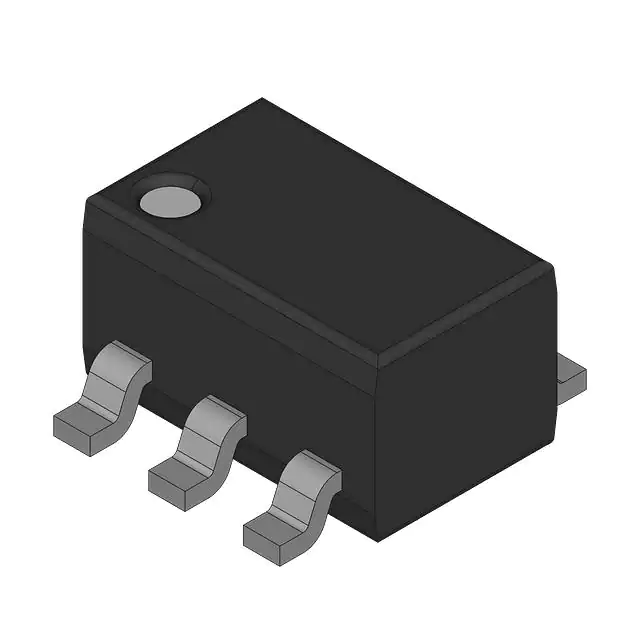
Renesas UPC2756TB-E3-A
- Part No.:
- UPC2756TB-E3-A
- Manufacturer:
- Renesas
- Category:
- RF Mixers
- Package:
- SOT-23-6 Thin, TSOT-23-6
- Datasheet:
-
 UPC2756TB-E3-A.pdf
- Description:
- RF/MICROWAVE UP/DOWN CONVERTER
- Quantity:
- Payment:

- Shipping:

Inventory:37,099
Please send an inquiry. Send us your inquiry, and we will respond immediately.
Product details
Overview
UPC2756TB-E3-A from NEC (now Renesas) is a silicon MMIC L-band downconverter IC integrating a double-balanced mixer, IF amplifier, and on-board LO oscillator in a single 6-pin SOT-363 package. It delivers 14 dB typical conversion gain, 13 dB noise figure at 900 MHz RF/150 MHz IF, −8 dBm saturated output power, and +4 dBm OIP3 across 0.1–2.0 GHz RF and 10–300 MHz IF bands, operating from 2.7–3.3 V supply. It is used in wireless receiver front-ends requiring compact, self-contained frequency translation.
For engineers reviewing the UPC2756TB-E3-A datasheet, UPC2756TB-E3-A pinout, UPC2756TB-E3-A application, or UPC2756TB-E3-A equivalent, key selection considerations include its integrated LO architecture, 6-pin SOT-363 footprint, 3 V operation, RF-to-IF conversion performance across L-band, and thermal resistance of 325°C/W on standard PCB mounting.
Technical Context
The UPC2756TB-E3-A implements a monolithic double-balanced mixer core with built-in differential LO oscillator, eliminating external LO sources and reducing system component count. Its IF amplifier provides single-ended push-pull emitter-follower output with low impedance and DC-coupled biasing via internal transistor structure.
It operates as a superheterodyne downconverter with fixed LO generation enabled by external tank circuit (e.g., varactor diode + inductor), supporting both high-side and low-side injection. The device requires no external IF filtering or LO buffering, and all RF/IF ports are matched to 50 Ω under specified conditions.
Key Specifications
| Parameter | Value and Actual Design Meaning |
|---|---|
| RF Frequency Range | 0.1–2.0 GHz - supports full L-band reception without external tuning components |
| IF Frequency Range | 10–300 MHz - enables baseband or intermediate frequency processing with standard IF filters |
| Conversion Gain | 14 dB typ. at 900 MHz RF/150 MHz IF - provides sufficient signal level for downstream IF amplification |
| Noise Figure | 13 dB max. at 900 MHz RF/150 MHz IF - maintains SNR integrity in weak-signal receiver stages |
| OIP3 | +4 dBm at fRF = 0.8–2.0 GHz - indicates moderate linearity suitable for narrowband wireless receivers |
| LO Leakage | −35 dBm at RF pin, −23 dBm at IF pin - minimizes self-interference and simplifies filtering requirements |
| Supply Voltage | 2.7–3.3 V - compatible with modern 3 V logic and battery-powered portable systems |
Pinout & Package
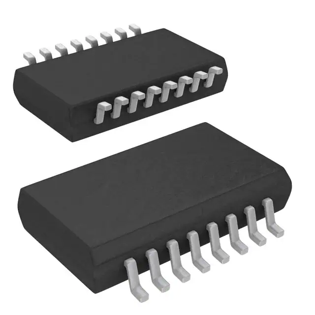
UPC2756TB-E3-A is housed in a 6-pin SOT-363 (Super Minimold) package, measuring 2.1 × 1.25 × 0.9 mm, with lead pitch of 0.65 mm and embossed tape packaging for automated assembly.
| Pin/Terminal | Circuit Role | Design Meaning |
|---|---|---|
| 1 - RFIN | RF Input | Signal input to double-balanced mixer; requires AC coupling capacitor; internally matched to ~50 Ω at 900 MHz |
| 2 - GND | Ground Reference | Common ground for RF, LO, and IF sections; must be connected with minimal inductance to system ground plane |
| 3 - LO1 | LO Oscillator Terminal 1 | One terminal of differential LO tank connection; requires blocking capacitor to external resonator (e.g., varactor + inductor) |
| 4 - LO2 | LO Oscillator Terminal 2 | Second terminal of differential LO tank; unused when external LO is applied (bypassed to ground) |
| 5 - VCC | Power Supply | 3 V supply input; requires local 0.1 µF bypass capacitor to suppress supply noise and stabilize LO operation |
| 6 - IFOUT | IF Output | Emitter-follower IF buffer output; low-impedance, single-ended; requires AC coupling to next stage |
Key Features
| Feature | Design Value |
|---|---|
| Integrated LO oscillator | Eliminates need for external LO source or synthesizer, reducing BOM count and board area in compact receivers |
| Double-balanced mixer topology | Provides inherent LO-to-RF and LO-to-IF isolation, minimizing spurious feedthrough and easing filter design |
| 6-pin SOT-363 package | Enables high-density surface mounting with industry-standard footprint and reflow compatibility |
| 3 V operation | Supports direct integration into 3 V battery-powered or low-voltage embedded systems without level-shifting |
| On-chip IF amplifier | Delivers buffered, low-Z IF output capable of driving 50 Ω loads without external gain stages |
Applications
| GPS/GLONASS Receivers | ISM Band Wireless Links |
|---|---|
|
Use Scenario: L-band satellite navigation front-end receiving 1.575 GHz GPS L1 signals with 150 MHz IF translation. IC Role / Device Role / Timing Role: Downconverter IC performing RF-to-IF translation with integrated LO generation and IF amplification. Use Value: Reduces component count by replacing discrete mixer + LO + IF amp with single chip, lowering PCB area and power consumption. |
Use Scenario: 902–928 MHz ISM band transceiver receiver path in industrial telemetry modules. IC Role / Device Role / Timing Role: Self-contained downconverter translating RF to 70 MHz IF for ADC sampling and digital demodulation. Use Value: Enables rapid prototyping and production of compact, low-cost receivers without external LO design effort. |
| Cellular Infrastructure Monitoring | Wireless Security Sensors |
|
Use Scenario: Spectrum monitoring unit detecting GSM 900 MHz uplink activity using 100 MHz IF output. IC Role / Device Role / Timing Role: RF front-end downconverter providing stable gain and noise performance across temperature range. Use Value: Maintains consistent sensitivity from −40°C to +85°C due to integrated biasing and thermal design. |
Use Scenario: Battery-operated door/window sensor receiving 433 MHz ASK/OOK signals with 10–50 MHz IF output. IC Role / Device Role / Timing Role: Low-power L-band downconverter enabling long-life operation with 3 V supply and <8 mA ICC. Use Value: Achieves >1-year battery life in intermittent-receive mode while preserving signal fidelity for envelope detection. |
Equivalent & Alternatives
The following parts are listed as comparable options for similar downconverter applications.
| Alternative Part | Technical Difference | Application Difference | Selection Advice |
|---|---|---|---|
| UPC2756T-E3-A | Larger SOIC-8 package; identical electrical specs but higher thermal resistance (380°C/W vs. 325°C/W) | Requires more PCB area; less suitable for ultra-compact designs | Select UPC2756T-E3-A only if SOIC-8 handling or legacy layout reuse is required |
| MAX2682EUT+T | 3 V, 400–2500 MHz RF range; 13.5 dB gain; 10.5 dB NF; no integrated LO - requires external LO source | Needs external PLL/synthesizer; higher system-level integration effort but wider RF bandwidth | Select MAX2682EUT+T when wideband coverage beyond 2 GHz or external LO control is needed |
Compared with UPC2756T-E3-A, the UPC2756TB-E3-A saves board space and improves thermal performance; compared with MAX2682EUT+T, it reduces system complexity by integrating the LO but trades off RF bandwidth and external LO flexibility.
Availability
UPC2756TB-E3-A is available at Aetrix Electronics and suitable for GPS receivers, ISM band wireless links, cellular infrastructure monitoring, and wireless security sensors requiring stable component supply and RoHS-compliant, Pb-free packaging.
Supply support for UPC2756TB-E3-A includes scheduled delivery planning, volume procurement assistance, BOM continuity management, traceable sourcing, and lifecycle availability coordination for OEM customers, industrial embedded developers, connected-device designers, and electronics production programs.
Manufacturer
Renesas Electronics (formerly NEC Electronics) is a global semiconductor leader specializing in microcontrollers, analog, and RF solutions, with rigorous quality assurance and automotive-grade reliability standards.
The UPC2756TB-E3-A belongs to NEC's silicon MMIC downconverter product line, designed specifically for compact, low-power L-band wireless receiver front-ends where integration, size, and supply simplicity are critical.
FAQ
What is the function of pins 3 and 4 (LO1 and LO2) on the UPC2756TB-E3-A?
Pins 3 and 4 serve as the differential terminals of the internal LO oscillator. When used in self-oscillating mode, they connect to an external tank circuit (e.g., varactor diode and inductor) to set the LO frequency. If an external LO is supplied, one pin is used as input and the other is bypassed to ground via a capacitor. The UPC2756TB-E3-A relies on this configuration to generate its own LO signal without requiring a separate synthesizer.
Does the UPC2756TB-E3-A require external matching networks at RF or IF ports?
No - the UPC2756TB-E3-A is internally matched to 50 Ω at RF and IF ports under standard test conditions (VCC = 3.0 V, TA = 25°C). Application circuits confirm use of only DC-blocking capacitors and bypass capacitors; no external baluns, transformers, or impedance-matching stubs are required for nominal operation across its specified frequency ranges.
What is the maximum RF input power the UPC2756TB-E3-A can handle before compression?
The UPC2756TB-E3-A exhibits −8 dBm saturated output power (PSAT) at 900 MHz RF/150 MHz IF with −10 dBm RF input. Compression begins near −20 dBm RF input, where conversion gain drops ~1 dB. Therefore, linear operation is maintained up to approximately −25 dBm RF input for minimal distortion, making the UPC2756TB-E3-A suitable for low-level signal reception rather than high-power mixing.
Is the UPC2756TB-E3-A pin-compatible with any other NEC/Renesas downconverter ICs?
Yes - the UPC2756TB-E3-A is explicitly documented as pin-compatible with the larger UPC2756T (SOIC-8), sharing identical pin functions and electrical behavior. This allows drop-in replacement in existing layouts where space permits the SOT-363 variant, enabling miniaturization without redesigning the signal routing or power delivery network for the UPC2756TB-E3-A.
What is the phase noise performance of the integrated LO in the UPC2756TB-E3-A?
The UPC2756TB-E3-A achieves −68 dBc/Hz phase noise at 10.2 kHz offset from a 1.9 GHz LO carrier, measured at pin 6 (IFOUT) under VCC = 3 V and TA = +25°C. This level supports adequate adjacent-channel rejection in narrowband receivers such as GPS and ISM applications, though not suitable for high-order QAM or wideband OFDM systems requiring sub-−80 dBc/Hz performance.
UPC2756TB-E3-A Specifications
- Product attributes
- Attribute value
- Manufacturer:
- Renesas
- Series:
- UPB2756TB
- Package/Case:
- SOT-23-6 Thin, TSOT-23-6
- Packaging:
- Bulk
- Product Status:
- Obsolete
- RF Type:
- -
- Frequency:
- 100MHz ~ 2GHz
- Number of Mixers:
- 1
- Gain:
- 14dB
- Noise Figure:
- 13dB
- Secondary Attributes:
- Down Converter
- Current - Supply:
- 8mA
- Voltage - Supply:
- 2.7V ~ 3.3V
- Mounting Type:
- Surface Mount
- Supplier Device Package:
- 6-SuperMiniMold
UPC2756TB-E3-A FAQ
1.How can I place an order for UPC2756TB-E3-A through Aetrix?
Please submit a Request for Quotation (RFQ) for UPC2756TB-E3-A on Aetrix. Our sales agent will provide a competitive quotation and guide you through the order confirmation once you accept the terms.
2.Are the price and stock information for UPC2756TB-E3-A reliable?
The price and inventory of UPC2756TB-E3-A are updated periodically and may fluctuate due to market conditions. Stock and pricing data are typically refreshed every 24 hours. Quotation validity for UPC2756TB-E3-A is usually 5 days.
3.What payment methods are accepted for UPC2756TB-E3-A?
We accept Wire Transfer, PayPal, Credit Card, Western Union, MoneyGram, and Escrow for UPC2756TB-E3-A transactions.
Note: Certain payment methods may incur a processing fee.
4.How is shipping managed for UPC2756TB-E3-A?
UPC2756TB-E3-A orders can be shipped via leading logistics carriers, including DHL, UPS, FedEx, TNT, or Registered Mail.
Once your UPC2756TB-E3-A order is processed, you will receive an email with the shipment details and tracking number.
Note: Tracking information may take up to 24 hours to appear. Express delivery typically takes 3–5 business days.
5.How can I obtain technical support or documentation for UPC2756TB-E3-A?
For technical support, including UPC2756TB-E3-A datasheets, pinout diagrams, or application guidance, please contact our engineering support team. They can provide detailed documentation and assistance for your UPC2756TB-E3-A requirements.
6.How does Aetrix verify that UPC2756TB-E3-A is sourced from the original manufacturer or authorized distributors?
All UPC2756TB-E3-A products on Aetrix are procured from qualified distributors and authorized channels. Our dedicated quality assurance team conducts strict verification, including traceability checks and, if necessary, third-party testing. This ensures that UPC2756TB-E3-A meets industry standards.
7.What is the process for return or replacement of UPC2756TB-E3-A?
All UPC2756TB-E3-A units undergo pre-shipment inspection (PSI). If there is an issue with UPC2756TB-E3-A, returns or replacements are accepted under the following conditions:
1.Quantity discrepancies, incorrect items, or visible external defects (such as breakage or corrosion), acknowledged by Aetrix.
2.The issue is reported within 90 days of delivery.
3.The UPC2756TB-E3-A part is unused and in its original packaging.
Return procedure for UPC2756TB-E3-A:
1.Submit a request within 90 days.
2.Obtain a Return Material Authorization (RMA) from Aetrix.
UPC2756TB-E3-A Tags
-
MAX2671EUT+T
Analog Devices Inc./Maxim Integrated

-
ADEX-10+
Mini-Circuits
-
ADE-2+
Mini-Circuits
-
ADE-1+
Mini-Circuits
-
LT5560EDD#PBF
Analog Devices Inc.
-
LT5560EDD#TRPBF
Analog Devices Inc.

-
LTC5562IUC#TRPBF
Analog Devices Inc.
-
MAX2681EUT+T
Analog Devices Inc./Maxim Integrated
-
ADE-1ASK+
Mini-Circuits
-
ADE-1L+
Mini-Circuits
-
ADL5350ACPZ-R7
Analog Devices Inc.
-
AD608ARZ-RL
Analog Devices Inc.
Tech Hub

TTL and CMOS logic families differ in thresholds, loading, output drive, power and timing. This engineering guide compares 74HC and 74HCT, calculates noise margins and checks 3.3 V/5 V compatibility.

A practical engineering guide to 3.3V and 5V logic compatibility, input thresholds, resistor dividers, translator ICs, MOSFET level shifting, I2C pull-ups, timing limits and power-sequencing risks.

The 74HC595 uses push-pull logic outputs, while the TPIC6B595 uses 50 V open-drain DMOS sinks for higher-power loads. This guide compares timing, current limits, 3.3 V interfacing, load wiring, thermal…

The 74HC595 converts serial data into eight stable parallel outputs. This guide covers pin functions, shift and storage timing, OE and MR behavior, drive-current limits, cascading, voltage compatibilit…

A technical comparison of level-sensitive latches and edge-triggered flip-flops, covering timing windows, setup and hold limits, master–slave operation, time borrowing, race-through, HDL inference and…

A D latch stores one bit while Enable controls when data can pass. This reference covers gate-level operation, truth tables, transparency, setup and hold timing, LE versus OE, common ICs and practical …

An SR latch stores one bit through cross-coupled feedback. This engineering reference covers NOR and NAND implementations, truth tables, forbidden-state recovery, gated operation, switch debouncing, fa…

Latch circuits retain one bit through feedback. This technical reference covers SR and D latches, truth tables, transparency, timing limits, latch-versus-flip-flop behavior, applications and common log…

An engineering guide to LED driver operation, constant-current and constant-voltage outputs, linear and switching topologies, dimming, IC selection, calculations, replacement compatibility, and fault c…

Operational amplifier guide covering op amp basics, feedback, ideal vs real op amps, common configurations, buffer circuits, offset, bias current, gain-bandwidth, slew rate, rail-to-rail limits and sel…


