
 My Inquiry
 My Account


Renesas UPD30541GD-200-WML-A
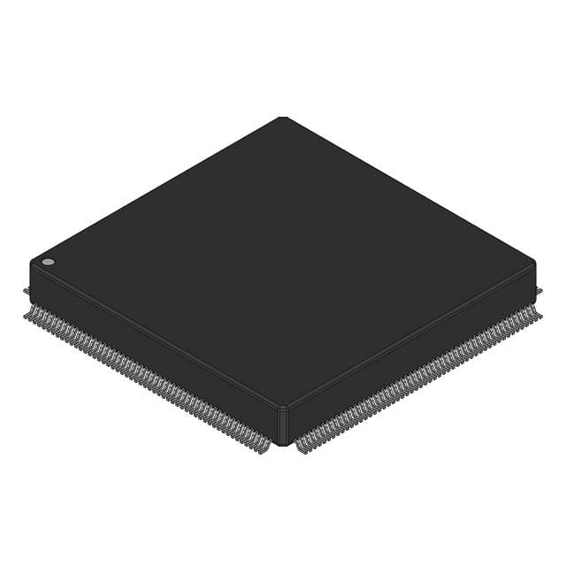
- Part No.:
- UPD30541GD-200-WML-A
- Manufacturer:
- Renesas
- Category:
- Microprocessors
- Package:
- -
- Datasheet:
-
 UPD30541GD-200-WML-A.pdf
- Description:
- RISC MICROPROCESSOR, 64-BIT
- Quantity:
- Payment:

- Shipping:

Inventory:1,317
Please send an inquiry. Send us your inquiry, and we will respond immediately.
Product details
Overview
UPD30541GD-200-WML-A from NEC Electronics is a 64-bit MIPS IV-compliant RISC microprocessor operating at 200 MHz, featuring symmetric dual-issue superscalar pipeline with six independent execution units, 32 KB instruction and 32 KB data caches with line locking, and on-chip JTAG/N-wire/N-trace debugging - deployed in digital set-top boxes for real-time video decoding and system control.
For engineers reviewing the UPD30541GD-200-WML-A datasheet, UPD30541GD-200-WML-A pinout, UPD30541GD-200-WML-A application, or UPD30541GD-200-WML-A equivalent, key selection criteria include MIPS IV ISA compliance, 200 MHz clock rate with 377 Dhrystone MIPS performance, 208-pin PQFP package thermal profile, and support for integer MAC and packed data vector operations in embedded multimedia systems.
Technical Context
The UPD30541GD-200-WML-A implements a symmetric two-way superscalar pipeline with two unified 64-bit integer/floating-point units and 64-bit barrel shifters. It supports variable-page-size virtual memory mapping via a 48-entry joint TLB and separate four-entry micro-TLBs for instructions and data.
Cache subsystem includes nonblocking load/store architecture with up to four outstanding data cache misses and concurrent cache fill capability. The SysAD bus operates at 100 MHz with 32-bit multiplexed address/data interface and full MIPS IV instruction set extensions including rotate, integer MAC, and packed 8×8-bit vector operations.
Key Specifications
| Parameter | Value and Actual Design Meaning |
|---|---|
| Max Operating Frequency | 200 MHz - enables 377 Dhrystone MIPS throughput for real-time multimedia processing. |
| Instruction Set Architecture | MIPS IV-compliant - supports integer multiply-accumulate, rotate, and packed data vector instructions for DSP and image acceleration. |
| Cache Configuration | 32 KB two-way set-associative instruction + 32 KB two-way set-associative data cache with line locking - ensures deterministic latency for critical firmware and video buffers. |
| TLB Architecture | 48-entry joint instruction/data TLB + separate 4-entry micro-TLBs - optimizes virtual-to-physical address translation for mixed instruction/data access patterns. |
| Power Consumption (typ.) | 2.1 W at 200 MHz - achieved via gated clock and low-switching circuit design suitable for fanless STB enclosures. |
| Bus Interface | 32-bit multiplexed SysAD bus @ 100 MHz - provides 800 MB/s peak bandwidth for high-throughput video frame transfers. |
| Debug Support | On-chip JTAG, N-wire, and N-trace - enables real-time trace capture and hardware breakpoints without external probes. |
Pinout & Package
UPD30541GD-200-WML-A is housed in a 208-pin Plastic Quad Flat Package (PQFP) with 0.65 mm lead pitch, designed for surface-mount assembly and thermal dissipation in compact consumer electronics enclosures.
| Pin/Terminal | Circuit Role | Design Meaning |
|---|---|---|
| VDD, VSS | Core power supply and ground | Dual 3.3 V domains (I/O and core) with dedicated decoupling pads per power group. |
| CLKIN | Primary clock input | Accepts single-ended 200 MHz reference; internal PLL generates internal core clock. |
| SYSAD[31:0] | Multiplexed address/data bus | Time-multiplexed 32-bit bus supporting burst transfers and pipelined read/write cycles. |
| RESET#, NMI#, INT[7:0]# | System control and interrupt inputs | Asynchronous reset with configurable NMI and eight vectored interrupt lines for peripheral prioritization. |
| TDO, TDI, TCK, TMS | JTAG boundary-scan interface | Fully compliant IEEE 1149.1 interface for production test and in-system debug access. |
Key Features
| Feature | Design Value |
|---|---|
| Dual-issue superscalar pipeline | Executes ALU, FP, and rotate instructions in parallel across six independent units - sustains >1.8 IPC in media workloads. |
| Cache line locking | Prevents eviction of critical OS kernel code or video decode buffers - eliminates cache-related jitter in real-time tasks. |
| Integer MAC and vector ops | Hardware-accelerated 32-bit integer multiply-accumulate and 8×8-bit packed data operations - offloads DSP functions from main thread. |
| Nonblocking cache misses | Supports up to four outstanding data cache misses - maintains instruction flow during large buffer accesses typical in MPEG-2 decoding. |
| Variable-page-size TLB | Enables efficient mapping of both small (4 KB) and large (4 MB) memory pages - reduces TLB pressure in multi-tasking STB environments. |
Applications
| Digital Set-Top Box | Internet Appliance |
|---|---|
Use Scenario: Real-time MPEG-2 video decode, EPG navigation, and conditional access management in cable/satellite receivers. IC Role / Device Role / Timing Role: Primary application processor executing middleware, demux, and decode firmware with deterministic interrupt latency. Use Value: 377 Dhrystone MIPS and packed vector ops enable smooth 1080i playback while running Linux-based UI stack. | Use Scenario: Web browsing, email, and Java applet execution in network-connected home terminals. IC Role / Device Role / Timing Role: System-on-chip host CPU managing Ethernet MAC, flash storage, and LCD controller interfaces. Use Value: 200 MHz clock and 32 KB caches deliver responsive UI rendering and TCP/IP stack throughput without external cache SRAM. |
| Office Automation Equipment | Networked Media Player |
Use Scenario: Document scanning, OCR preprocessing, and print job spooling in multifunction peripherals. IC Role / Device Role / Timing Role: Embedded controller coordinating scanner sensor timing, JPEG compression, and USB host protocol stack. Use Value: Integer MAC and rotate instructions accelerate bitmap rotation and binarization algorithms in real time. | Use Scenario: Local video streaming from USB mass storage or network shares with subtitle overlay and audio mixing. IC Role / Device Role / Timing Role: Media processing engine handling transport stream demux, H.264 decode, and stereo DAC interface timing. Use Value: Nonblocking cache and dual FP units sustain 30 fps 720p decode while buffering network packets and rendering OSD graphics. |
Equivalent & Alternatives
The following parts are listed as comparable options for similar 64-bit embedded RISC processor applications.
| Alternative Part | Technical Difference | Application Difference | Selection Advice |
|---|---|---|---|
| VR5432 µPD30541GD-167-WML | 167 MHz max frequency; 316 Dhrystone MIPS; same 208-pin PQFP package and instruction set. | Lower thermal envelope (1.8 W) but reduced throughput for HD video decode pipelines. | Select when power budget is constrained and 1080i decode is not required. |
| MIPS Technologies RM5261 | 200 MHz, 32 KB I-cache/32 KB D-cache, but lacks packed data vector and integer MAC extensions. | Compatible for general-purpose Linux execution but unsuitable for accelerated multimedia workloads. | Choose only if application does not require DSP or image processing acceleration. |
Compared with µPD30541GD-167-WML and RM5261, the UPD30541GD-200-WML-A delivers highest sustained MIPS/Watt in its class and unique hardware support for 8×8-bit packed operations - making it the only option among the three capable of real-time MPEG-2 and JPEG acceleration without coprocessor assistance.
Availability
UPD30541GD-200-WML-A is available at Aetrix Electronics and suitable for digital set-top boxes, Internet appliances, and office automation equipment requiring stable component supply across long-lifecycle consumer electronics programs.
Supply support for UPD30541GD-200-WML-A includes scheduled delivery planning, volume procurement assistance, BOM continuity management, traceable sourcing, and lifecycle availability coordination for OEM customers, industrial embedded developers, connected-device designers, and electronics production programs.
Manufacturer
NEC Electronics Inc. was a leading Japanese semiconductor manufacturer specializing in high-performance microprocessors, memory, and analog ICs before its merger into Renesas Electronics in 2010.
The VR5432 family, including UPD30541GD-200-WML-A, was engineered for cost-sensitive, high-throughput embedded multimedia systems - balancing MIPS IV compute density, low-power operation, and integrated debug infrastructure for rapid STB development.
FAQ
What is the maximum operating frequency of the UPD30541GD-200-WML-A?
The UPD30541GD-200-WML-A is rated for a maximum operating frequency of 200 MHz, delivering 377 Dhrystone MIPS performance. This frequency is guaranteed under specified voltage (3.3 V ±0.3 V) and temperature (0°C to 70°C) conditions per NEC's original datasheet. The part uses an internal PLL to generate the core clock from the external CLKIN signal, and timing closure requires strict adherence to setup/hold margins on the SysAD bus.
Does the UPD30541GD-200-WML-A support hardware debugging features?
Yes, the UPD30541GD-200-WML-A integrates full IEEE 1149.1 JTAG, NEC-specific N-wire, and N-trace debugging interfaces. These enable real-time instruction trace, hardware breakpoints, and on-chip watchpoint monitoring without halting system execution. The UPD30541GD-200-WML-A also includes performance counters that track any two of 16 selectable events for software optimization.
What package type is used for the UPD30541GD-200-WML-A?
The UPD30541GD-200-WML-A is packaged in a 208-pin Plastic Quad Flat Package (PQFP) with 0.65 mm lead pitch and standard JEDEC MO-118 footprint. This package supports reflow soldering and provides adequate thermal dissipation for its 2.1 W typical power consumption in ventilated consumer enclosures.
Is the UPD30541GD-200-WML-A compatible with the MIPS III instruction set?
No, the UPD30541GD-200-WML-A implements the MIPS IV instruction set architecture exclusively. While it maintains backward compatibility with MIPS III user-mode instructions, it adds mandatory extensions including integer multiply-accumulate, rotate, and packed data vector operations. Code compiled for MIPS III may execute but cannot leverage UPD30541GD-200-WML-A's performance-critical acceleration features.
What are the cache characteristics of the UPD30541GD-200-WML-A?
The UPD30541GD-200-WML-A features separate 32 KB two-way set-associative instruction and data caches, each with parity protection and programmable line locking. Cache line size is 32 bytes, and the nonblocking architecture allows up to four outstanding data cache misses. Both caches support write-back policy and can be locked to prevent eviction of critical OS or video buffers.
UPD30541GD-200-WML-A Specifications
- Product attributes
- Attribute value
- Manufacturer:
- Renesas
- Package/Case:
- -
- Series:
- *
- Packaging:
- Bulk
- Product Status:
- Active
- Core Processor:
- -
- Number of Cores/Bus Width:
- -
- Speed:
- -
- Co-Processors/DSP:
- -
- RAM Controllers:
- -
- Graphics Acceleration:
- -
- Display & Interface Controllers:
- -
- Ethernet:
- -
- SATA:
- -
- USB:
- -
- Voltage - I/O:
- -
- Operating Temperature:
- -
- Grade:
- -
- Qualification:
- -
- Security Features:
- -
- Mounting Type:
- -
- Supplier Device Package:
- -
- Additional Interfaces:
- -
UPD30541GD-200-WML-A FAQ
1.How can I place an order for UPD30541GD-200-WML-A through Aetrix?
Please submit a Request for Quotation (RFQ) for UPD30541GD-200-WML-A on Aetrix. Our sales agent will provide a competitive quotation and guide you through the order confirmation once you accept the terms.
2.Are the price and stock information for UPD30541GD-200-WML-A reliable?
The price and inventory of UPD30541GD-200-WML-A are updated periodically and may fluctuate due to market conditions. Stock and pricing data are typically refreshed every 24 hours. Quotation validity for UPD30541GD-200-WML-A is usually 5 days.
3.What payment methods are accepted for UPD30541GD-200-WML-A?
We accept Wire Transfer, PayPal, Credit Card, Western Union, MoneyGram, and Escrow for UPD30541GD-200-WML-A transactions.
Note: Certain payment methods may incur a processing fee.
4.How is shipping managed for UPD30541GD-200-WML-A?
UPD30541GD-200-WML-A orders can be shipped via leading logistics carriers, including DHL, UPS, FedEx, TNT, or Registered Mail.
Once your UPD30541GD-200-WML-A order is processed, you will receive an email with the shipment details and tracking number.
Note: Tracking information may take up to 24 hours to appear. Express delivery typically takes 3–5 business days.
5.How can I obtain technical support or documentation for UPD30541GD-200-WML-A?
For technical support, including UPD30541GD-200-WML-A datasheets, pinout diagrams, or application guidance, please contact our engineering support team. They can provide detailed documentation and assistance for your UPD30541GD-200-WML-A requirements.
6.How does Aetrix verify that UPD30541GD-200-WML-A is sourced from the original manufacturer or authorized distributors?
All UPD30541GD-200-WML-A products on Aetrix are procured from qualified distributors and authorized channels. Our dedicated quality assurance team conducts strict verification, including traceability checks and, if necessary, third-party testing. This ensures that UPD30541GD-200-WML-A meets industry standards.
7.What is the process for return or replacement of UPD30541GD-200-WML-A?
All UPD30541GD-200-WML-A units undergo pre-shipment inspection (PSI). If there is an issue with UPD30541GD-200-WML-A, returns or replacements are accepted under the following conditions:
1.Quantity discrepancies, incorrect items, or visible external defects (such as breakage or corrosion), acknowledged by Aetrix.
2.The issue is reported within 90 days of delivery.
3.The UPD30541GD-200-WML-A part is unused and in its original packaging.
Return procedure for UPD30541GD-200-WML-A:
1.Submit a request within 90 days.
2.Obtain a Return Material Authorization (RMA) from Aetrix.
UPD30541GD-200-WML-A Tags

-
AT91SAM9260B-CU-999
Microchip Technology
-
AT91SAM9G25-CU
Microchip Technology

-
ATSAMA5D27C-CU
Microchip Technology
-
AT91SAM9X35-CU
Microchip Technology
-
AT91SAM9X25-CU
Microchip Technology

-
MCIMX6Y2CVM08AB
NXP Semiconductors
.JPG)
-
AM3352BZCZ100
Texas Instruments
-
AT91SAM9260B-CU
Microchip Technology

-
AT91SAM9260B-QU
Microchip Technology

-
ATSAMA5D31A-CU
Microchip Technology
-
AT91SAM9G20B-CU-999
Microchip Technology
-
MCIMX6Y2CVM05AB
NXP Semiconductors
Tech Hub

TTL and CMOS logic families differ in thresholds, loading, output drive, power and timing. This engineering guide compares 74HC and 74HCT, calculates noise margins and checks 3.3 V/5 V compatibility.

A practical engineering guide to 3.3V and 5V logic compatibility, input thresholds, resistor dividers, translator ICs, MOSFET level shifting, I2C pull-ups, timing limits and power-sequencing risks.

The 74HC595 uses push-pull logic outputs, while the TPIC6B595 uses 50 V open-drain DMOS sinks for higher-power loads. This guide compares timing, current limits, 3.3 V interfacing, load wiring, thermal…

The 74HC595 converts serial data into eight stable parallel outputs. This guide covers pin functions, shift and storage timing, OE and MR behavior, drive-current limits, cascading, voltage compatibilit…

A technical comparison of level-sensitive latches and edge-triggered flip-flops, covering timing windows, setup and hold limits, master–slave operation, time borrowing, race-through, HDL inference and…

A D latch stores one bit while Enable controls when data can pass. This reference covers gate-level operation, truth tables, transparency, setup and hold timing, LE versus OE, common ICs and practical …

An SR latch stores one bit through cross-coupled feedback. This engineering reference covers NOR and NAND implementations, truth tables, forbidden-state recovery, gated operation, switch debouncing, fa…

Latch circuits retain one bit through feedback. This technical reference covers SR and D latches, truth tables, transparency, timing limits, latch-versus-flip-flop behavior, applications and common log…

An engineering guide to LED driver operation, constant-current and constant-voltage outputs, linear and switching topologies, dimming, IC selection, calculations, replacement compatibility, and fault c…

Operational amplifier guide covering op amp basics, feedback, ideal vs real op amps, common configurations, buffer circuits, offset, bias current, gain-bandwidth, slew rate, rail-to-rail limits and sel…


