
 My Inquiry
 My Account


Renesas UPD44325182BF5-E40-FQ1-A
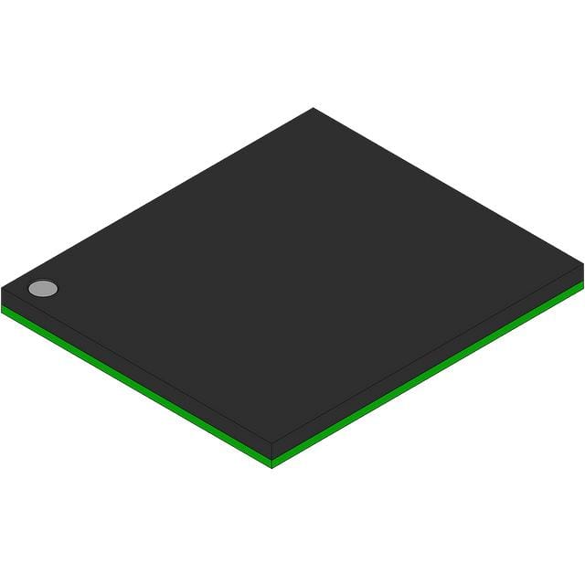
- Part No.:
- UPD44325182BF5-E40-FQ1-A
- Manufacturer:
- Renesas
- Category:
- Memory
- Package:
- 165-FBGA
- Datasheet:
-
 UPD44325182BF5-E40-FQ1-A.pdf
- Description:
- IC SRAM 36MBIT PAR 165FBGA
- Quantity:
- Payment:

- Shipping:

Inventory:6,546
Please send an inquiry. Send us your inquiry, and we will respond immediately.
Product details
Overview
UPD44325182BF5-E40-FQ1-A from Renesas Electronics is a 2,097,152-word × 18-bit synchronous Quad Data Rate II (QDR II) SRAM with 4.0 ns clock cycle time (250 MHz), 1.8 V core supply, HSTL interface, and 165-pin plastic BGA (15 × 17) package. It supports concurrent read/write operations, burst-2 DDR transactions, and is used in high-bandwidth networking buffers and packet forwarding engines.
For engineers reviewing the UPD44325182BF5-E40-FQ1-A datasheet, UPD44325182BF5-E40-FQ1-A pinout, UPD44325182BF5-E40-FQ1-A application, or UPD44325182BF5-E40-FQ1-A equivalent, key selection considerations include its 2M × 18 organization, 250 MHz QDR II timing, HSTL I/O compliance, PLL-enabled output clock alignment, and user-programmable output impedance (35–70 Ω).
Technical Context
This device implements a dual-port synchronous architecture with independent read and write data paths, enabling true concurrent access without arbitration overhead. Its burst-2 operation delivers two words per clock cycle on both ports, achieving 100% bus utilization under DDR timing.
The internal PLL synchronizes C/C# output clocks to K/K# inputs for precise flight-time matching, while DLL# allows PLL bypass during debug. Echo clocks CQ/CQ# provide tightly matched data-valid timing references, and ZQ enables dynamic output impedance calibration against system trace impedance.
Key Specifications
| Parameter | Value and Actual Design Meaning |
|---|---|
| Memory Organization | 2,097,152 words × 18 bits - provides 36 Mbit density with wide data path for burst-2 packet buffering |
| Clock Cycle Time | 4.0 ns - supports 250 MHz operation with guaranteed timing margins across industrial temperature range |
| Supply Voltage | VDD = 1.8 ± 0.1 V, VDDQ = 1.4–1.8 V - dual-rail design isolates core logic from I/O drivers to reduce noise coupling |
| Interface Standard | HSTL Class I - ensures compatibility with FPGA and ASIC memory controllers using 1.5 V I/O swing and VREF-based input thresholds |
| Output Impedance | User-programmable 35–70 Ω via ZQ pin - enables trace impedance matching without external termination resistors |
| Operating Temperature | 0 °C to +70 °C - validated for commercial/industrial embedded systems requiring stable timing at full speed |
| Package | 165-pin plastic BGA (15 × 17 mm) - standard footprint compatible with automated PCB assembly and thermal management |
Pinout & Package
165-pin plastic BGA (15 × 17 mm) with 0.8 mm pitch; top-side index mark per JEDEC MO-270. Package includes dedicated HSTL-compatible power (VDD, VDDQ), ground (VSS), reference (VREF), and impedance calibration (ZQ) pins.
| Pin/Terminal | Circuit Role | Design Meaning |
|---|---|---|
| K, K# | Input clock pair | Registers address/control on K rising edge and write data on K# rising edge; phase-aligned 180° differential pair required for timing closure |
| C, C# | Output clock pair | Controls output data timing; rising edges define valid windows for Q0–Q17; must be tied HIGH if using K/K# as output reference |
| CQ, CQ# | Echo clock outputs | Matched to Q outputs within ±0.35 ns; remain active during tristate and provide hardware-validated data-ready signal |
| R#, W# | Read/write strobes | Active-low synchronous commands; both high = NOP; setup/hold referenced to K rising edge only |
| BW0#, BW1# | Byte write enables | Select D0–D8 or D9–D17 for partial writes; independent control per burst word enables efficient sub-word updates |
| ZQ | Impedance calibration input | Connects to external resistor to ground; sets Q/CQ/CQ# output drive strength to 0.2 × RQ for controlled 35–70 Ω range |
| DLL# | PLL disable | Pull HIGH for normal operation; pull LOW to bypass PLL during low-frequency debug - AC specs not guaranteed |
| TMS, TDI, TCK, TDO | JTAG 1149.1 interface | 1.8 V I/O level test access port; TCK must tie to VSS if unused; supports boundary-scan and device ID verification |
Key Features
| Feature | Design Value |
|---|---|
| Concurrent read/write ports | Enables simultaneous packet ingress/egress in switch fabric without arbitration latency or pipeline stalls |
| Burst-2 DDR operation | Delivers two 18-bit words per clock edge pair, doubling effective bandwidth versus single-data-rate SRAM |
| Programmable output impedance | Eliminates need for discrete series termination resistors, reducing BOM count and PCB area in high-speed routing |
| PLL-synchronized output clocks | Reduces clock skew between C/C# and Q outputs to <0.45 ns, simplifying timing closure in 250 MHz systems |
| Clock-stop capability | Enters low-power state with 20 μs recovery to full operation - supports dynamic power gating in bursty traffic scenarios |
Applications
| Network Packet Buffer | High-Speed Test Equipment |
|---|---|
Use Scenario: Storing incoming Ethernet frames in a Layer 2 switch before classification and forwarding. IC Role / Device Role / Timing Role: Dual-port QDR II SRAM serving as first-in-first-out (FIFO) buffer with separate read/write address spaces and burst-2 throughput. Use Value: 250 MHz DDR operation delivers 9 Gbps sustained bandwidth, enabling line-rate 10GbE packet buffering without backpressure. | Use Scenario: Capturing high-resolution waveform samples in automated test equipment with real-time pattern generation. IC Role / Device Role / Timing Role: High-density memory for deep sample storage, interfaced to FPGA logic implementing parallel compare and trigger functions. Use Value: Concurrent read/write allows simultaneous acquisition and analysis, eliminating memory contention bottlenecks in multi-channel test systems. |
| Baseband Processing Buffer | Industrial PLC Data Exchange |
Use Scenario: Temporary storage of OFDM symbol data between FFT processing stages in LTE/5G baseband units. IC Role / Device Role / Timing Role: Synchronous SRAM acting as ping-pong buffer between digital front-end and channel estimation blocks. Use Value: HSTL interface ensures clean signal integrity at 250 MHz, while programmable impedance matches PCB traces for minimal reflection-induced jitter. | Use Scenario: Exchanging deterministic I/O data between redundant CPU modules in safety-critical programmable logic controllers. IC Role / Device Role / Timing Role: Deterministic-access memory providing atomic read-modify-write cycles for shared process variables. Use Value: Clock-stop mode enables synchronized power-down of redundant channels without data loss, supporting SIL3-certified fail-safe transitions. |
Equivalent & Alternatives
The following parts are listed as comparable options for similar QDR II SRAM applications.
| Alternative Part | Technical Difference | Application Difference | Selection Advice |
|---|---|---|---|
| CY7C2663KV18-400BAXI | 400 MHz (2.5 ns), 2M × 18, same 165-pin BGA but requires 1.5 V VDDQ only | Higher speed but tighter voltage tolerance; less margin for VDDQ droop in noisy environments | Select when system clock exceeds 250 MHz and board layout supports stricter 1.5 V regulation |
| AS7C3256A-15JIN | Asynchronous 32K × 8 CMOS SRAM, 15 ns access, SOJ-32 package | No burst, no DDR, no PLL - simpler interface but 1/33rd bandwidth and incompatible pinout | Select only for legacy designs where QDR timing and concurrency are unnecessary and cost is primary constraint |
Compared with CY7C2663KV18-400BAXI and AS7C3256A-15JIN, UPD44325182BF5-E40-FQ1-A offers optimal balance of 250 MHz performance, industrial temperature support, and flexible 1.4–1.8 V VDDQ operation - making it suitable for new designs requiring reliable QDR II functionality without over-spec'ing speed or sacrificing voltage margin.
Availability
UPD44325182BF5-E40-FQ1-A is available at Aetrix Electronics and suitable for network packet buffering, high-speed test instrumentation, baseband processing, industrial PLC data exchange, and deterministic real-time control applications requiring stable component supply and long-term lifecycle support.
Supply support for UPD44325182BF5-E40-FQ1-A includes scheduled delivery planning, volume procurement assistance, BOM continuity management, traceable sourcing, and lifecycle availability coordination for OEM customers, industrial embedded developers, connected-device designers, and electronics production programs.
Manufacturer
Renesas Electronics Corporation is a global semiconductor manufacturer specializing in microcontrollers, analog, power, and memory solutions for automotive, industrial, and infrastructure markets.
The UPD44325182BF5-E40-FQ1-A belongs to Renesas' QDR II SRAM product line, designed specifically for high-throughput, low-latency buffering in networking, telecommunications, and test equipment where concurrent dual-port access and precise DDR timing are critical.
FAQ
What is the maximum operating frequency of the UPD44325182BF5-E40-FQ1-A?
The UPD44325182BF5-E40-FQ1-A is rated for 250 MHz operation, corresponding to a 4.0 ns clock cycle time. This specification is guaranteed across the full 0 °C to +70 °C ambient temperature range and includes timing margins for setup/hold, clock jitter, and output validity. The device achieves this using an internal PLL that locks to the K/K# input clock and generates aligned C/C# output clocks.
Does the UPD44325182BF5-E40-FQ1-A support byte-level write masking?
Yes, the UPD44325182BF5-E40-FQ1-A supports byte-level write masking via two dedicated inputs: BW0# and BW1#. These active-low signals enable selective writing of D0–D8 (BW0# low) or D9–D17 (BW1# low) during each burst-2 write cycle. Both signals must be high to inhibit all writes. This feature allows efficient partial-word updates without read-modify-write overhead.
How does the ZQ pin function on the UPD44325182BF5-E40-FQ1-A?
The ZQ pin on the UPD44325182BF5-E40-FQ1-A serves as the output impedance calibration input. When connected to a precision resistor (typically 200 Ω) to ground, it configures the drive strength of Q, CQ, and CQ# outputs to 0.2 × RQ - yielding a calibrated range of 35–70 Ω. This eliminates external series termination and adapts dynamically every 20 μs to compensate for voltage and temperature drift.
Can the UPD44325182BF5-E40-FQ1-A operate without its internal PLL?
Yes, the UPD44325182BF5-E40-FQ1-A can operate without the internal PLL by asserting DLL# low. In this mode, the device uses K/K# directly as output timing references instead of C/C#, bypassing the PLL lock requirement. However, AC electrical characteristics including timing parameters and jitter tolerance are not guaranteed in PLL-bypass mode - it is intended only for debug or low-frequency validation.
What is the purpose of the CQ and CQ# pins on the UPD44325182BF5-E40-FQ1-A?
The CQ and CQ# pins on the UPD44325182BF5-E40-FQ1-A are synchronous echo clocks that track Q0–Q17 output data edges with tight skew (<0.35 ns). They remain active even when Q outputs are tristated and provide hardware-verified data-valid timing references for receiving logic - eliminating reliance on clock-to-output delay calculations and simplifying timing closure in high-speed interfaces.
UPD44325182BF5-E40-FQ1-A Specifications
- Product attributes
- Attribute value
- Manufacturer:
- Renesas
- Series:
- -
- Package/Case:
- 165-FBGA
- Packaging:
- Tray
- Product Status:
- Obsolete
- Programmable:
- Not Verified
- Memory Type:
- Volatile
- Memory Format:
- SRAM
- Technology:
- SRAM - Synchronous, QDR II
- Memory Size:
- 36Mbit
- Memory Organization:
- 2M x 18
- Memory Interface:
- Parallel
- Clock Frequency:
- 250 MHz
- Write Cycle Time - Word, Page:
- 4ns
- Access Time:
- -
- Voltage - Supply:
- 1.7V ~ 1.9V
- Operating Temperature:
- 0°C ~ 70°C (TA)
- Grade:
- -
- Qualification:
- -
- Mounting Type:
- Surface Mount
- Supplier Device Package:
- 165-FBGA (15x17)
UPD44325182BF5-E40-FQ1-A FAQ
1.How can I place an order for UPD44325182BF5-E40-FQ1-A through Aetrix?
Please submit a Request for Quotation (RFQ) for UPD44325182BF5-E40-FQ1-A on Aetrix. Our sales agent will provide a competitive quotation and guide you through the order confirmation once you accept the terms.
2.Are the price and stock information for UPD44325182BF5-E40-FQ1-A reliable?
The price and inventory of UPD44325182BF5-E40-FQ1-A are updated periodically and may fluctuate due to market conditions. Stock and pricing data are typically refreshed every 24 hours. Quotation validity for UPD44325182BF5-E40-FQ1-A is usually 5 days.
3.What payment methods are accepted for UPD44325182BF5-E40-FQ1-A?
We accept Wire Transfer, PayPal, Credit Card, Western Union, MoneyGram, and Escrow for UPD44325182BF5-E40-FQ1-A transactions.
Note: Certain payment methods may incur a processing fee.
4.How is shipping managed for UPD44325182BF5-E40-FQ1-A?
UPD44325182BF5-E40-FQ1-A orders can be shipped via leading logistics carriers, including DHL, UPS, FedEx, TNT, or Registered Mail.
Once your UPD44325182BF5-E40-FQ1-A order is processed, you will receive an email with the shipment details and tracking number.
Note: Tracking information may take up to 24 hours to appear. Express delivery typically takes 3–5 business days.
5.How can I obtain technical support or documentation for UPD44325182BF5-E40-FQ1-A?
For technical support, including UPD44325182BF5-E40-FQ1-A datasheets, pinout diagrams, or application guidance, please contact our engineering support team. They can provide detailed documentation and assistance for your UPD44325182BF5-E40-FQ1-A requirements.
6.How does Aetrix verify that UPD44325182BF5-E40-FQ1-A is sourced from the original manufacturer or authorized distributors?
All UPD44325182BF5-E40-FQ1-A products on Aetrix are procured from qualified distributors and authorized channels. Our dedicated quality assurance team conducts strict verification, including traceability checks and, if necessary, third-party testing. This ensures that UPD44325182BF5-E40-FQ1-A meets industry standards.
7.What is the process for return or replacement of UPD44325182BF5-E40-FQ1-A?
All UPD44325182BF5-E40-FQ1-A units undergo pre-shipment inspection (PSI). If there is an issue with UPD44325182BF5-E40-FQ1-A, returns or replacements are accepted under the following conditions:
1.Quantity discrepancies, incorrect items, or visible external defects (such as breakage or corrosion), acknowledged by Aetrix.
2.The issue is reported within 90 days of delivery.
3.The UPD44325182BF5-E40-FQ1-A part is unused and in its original packaging.
Return procedure for UPD44325182BF5-E40-FQ1-A:
1.Submit a request within 90 days.
2.Obtain a Return Material Authorization (RMA) from Aetrix.
UPD44325182BF5-E40-FQ1-A Tags

-
M24C02-WMN6TP
STMicroelectronics

-
AT24C02C-XHM-T
Microchip Technology

-
AT21CS01-STUM10-T
Microchip Technology

-
AT24C02C-SSHM-T
Microchip Technology

-
24LC01BT-I/OT
Microchip Technology

-
M24C02-FMC6TG
STMicroelectronics
-
AT24CS02-SSHM-T
Microchip Technology

-
93LC46BT-I/OT
Microchip Technology
-
AT24C04C-SSHM-T
Microchip Technology

-
24LC01BT-I/SN
Microchip Technology
-
24AA02UIDT-I/OT
Microchip Technology

-
AT24C08C-STUM-T
Microchip Technology
Tech Hub

TTL and CMOS logic families differ in thresholds, loading, output drive, power and timing. This engineering guide compares 74HC and 74HCT, calculates noise margins and checks 3.3 V/5 V compatibility.

A practical engineering guide to 3.3V and 5V logic compatibility, input thresholds, resistor dividers, translator ICs, MOSFET level shifting, I2C pull-ups, timing limits and power-sequencing risks.

The 74HC595 uses push-pull logic outputs, while the TPIC6B595 uses 50 V open-drain DMOS sinks for higher-power loads. This guide compares timing, current limits, 3.3 V interfacing, load wiring, thermal…

The 74HC595 converts serial data into eight stable parallel outputs. This guide covers pin functions, shift and storage timing, OE and MR behavior, drive-current limits, cascading, voltage compatibilit…

A technical comparison of level-sensitive latches and edge-triggered flip-flops, covering timing windows, setup and hold limits, master–slave operation, time borrowing, race-through, HDL inference and…

A D latch stores one bit while Enable controls when data can pass. This reference covers gate-level operation, truth tables, transparency, setup and hold timing, LE versus OE, common ICs and practical …

An SR latch stores one bit through cross-coupled feedback. This engineering reference covers NOR and NAND implementations, truth tables, forbidden-state recovery, gated operation, switch debouncing, fa…

Latch circuits retain one bit through feedback. This technical reference covers SR and D latches, truth tables, transparency, timing limits, latch-versus-flip-flop behavior, applications and common log…

An engineering guide to LED driver operation, constant-current and constant-voltage outputs, linear and switching topologies, dimming, IC selection, calculations, replacement compatibility, and fault c…

Operational amplifier guide covering op amp basics, feedback, ideal vs real op amps, common configurations, buffer circuits, offset, bias current, gain-bandwidth, slew rate, rail-to-rail limits and sel…


