
 My Inquiry
 My Account


Renesas UPD78F9212CS-CAB-A
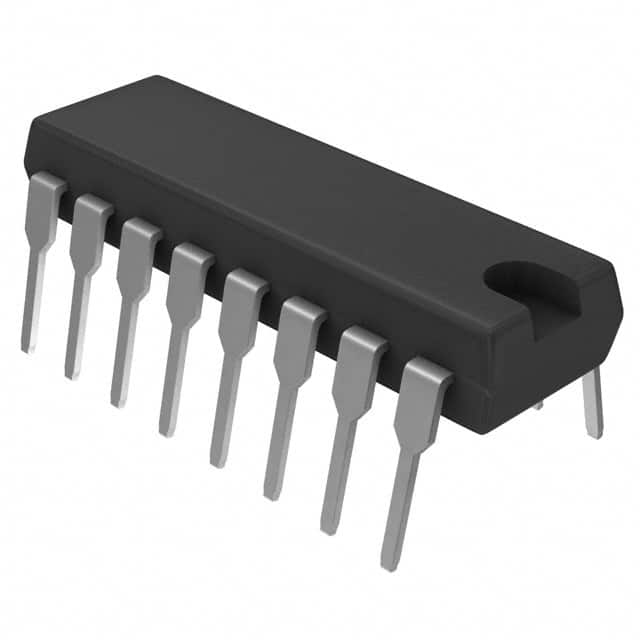
- Part No.:
- UPD78F9212CS-CAB-A
- Manufacturer:
- Renesas
- Category:
- Microcontrollers
- Package:
- 16-DIP (0.300", 7.62mm)
- Datasheet:
-
 UPD78F9212CS-CAB-A.pdf
- Description:
- IC MCU 8BIT 4KB FLASH
- Quantity:
- Payment:

- Shipping:

Inventory:1,701
Please send an inquiry. Send us your inquiry, and we will respond immediately.
Product details
Overview
UPD78F9212CS-CAB-A from Renesas Electronics is an 8-bit single-chip microcontroller in the 78K0S/KY1+ family, featuring 128 KB on-chip Flash memory, 8 KB RAM, and a 20 MHz max CPU clock. It integrates UART, I²C, 16-bit timer/counters, and 10-bit ADC with 16 channels. It targets industrial control panels requiring deterministic real-time response and low-power operation.
For engineers reviewing the UPD78F9212CS-CAB-A datasheet, UPD78F9212CS-CAB-A pinout, UPD78F9212CS-CAB-A application, or UPD78F9212CS-CAB-A equivalent, key selection criteria include Flash endurance (100k write/erase cycles), operating voltage range (2.7–5.5 V), package type (LQFP-100), and peripheral compatibility with legacy 78K0S designs.
Technical Context
The UPD78F9212CS-CAB-A implements the 78K0S CPU core with 16-bit addressing and 8-bit ALU, supporting 131 instructions including bit manipulation and multi-byte arithmetic. It uses SuperFlash® technology for program memory, enabling single-cycle read access and background operation during programming.
Clock generation includes a main system oscillator (1–20 MHz crystal), sub-oscillator (32.768 kHz), and on-chip PLL for internal clock multiplication. Reset sources comprise power-on reset, watchdog timer, and external reset pin - all mapped to dedicated SFR bits for software-controlled recovery.
Key Specifications
| Parameter | Value and Actual Design Meaning |
|---|---|
| Core Architecture | 78K0S 8-bit CPU with 16-bit address bus and 131-instruction set |
| Flash Memory | 128 KB on-chip SuperFlash®, 100k erase/write cycles, 100 µs byte write time |
| RAM Size | 8 KB on-chip SRAM, accessible in zero-wait-state mode at 20 MHz |
| Max Operating Frequency | 20 MHz CPU clock, supported by on-chip PLL with 1×–4× multiplication |
| Analog Peripherals | 10-bit ADC with 16 input channels, 1.2 µs conversion time, selectable reference (VDD or internal 2.5 V) |
| Digital Peripherals | 3 UARTs, 1 I²C interface, 4 16-bit timer/counters with capture/compare/PWM output |
| Supply Voltage Range | 2.7 V to 5.5 V - enables direct interface with 3.3 V logic and legacy 5 V systems |
Pinout & Package
LQFP-100 (14 mm × 14 mm, 0.5 mm pitch) with exposed thermal pad; RoHS-compliant, lead-free finish.
| Pin/Terminal | Circuit Role | Design Meaning |
|---|---|---|
| P00–P07 | Port 0 bidirectional I/O | Configurable as general-purpose I/O or multiplexed with UART0/INTP0–INTP3; supports pull-up/pull-down control |
| P20–P23 | Port 2 bidirectional I/O | Supports timer channel outputs (T0–T3), ADC trigger inputs, and external interrupt sources |
| P40–P47 | Port 4 bidirectional I/O | Primary ADC input channels (AN0–AN7); also usable as general I/O with programmable drive strength |
| X1/X2 | Crystal oscillator terminals | Accepts fundamental-mode quartz crystals from 1–20 MHz; internal load capacitors configurable via SFR |
| RESET | Active-low reset input | Asynchronous reset assertion clears CPU registers and halts execution; debounced internally for noise immunity |
Key Features
| Feature | Design Value |
|---|---|
| On-chip debug support | Fully integrated on-chip debug interface compatible with QB-MINI2 emulator - no external debug header required |
| Low-power modes | Four modes (HALT, STOP, SLOW, IDLE) with wake-up latency ≤ 2 µs from STOP mode via external interrupt or RTC alarm |
| Flash security | Read-out protection enabled via lock-bit configuration - prevents unauthorized firmware extraction during debugging |
| ADC self-test | Built-in calibration mode verifies ADC linearity and offset without external reference components |
| Peripheral clock gating | Individual enable/disable control per peripheral module reduces dynamic power consumption by up to 40% when unused |
Applications
| Industrial HMI Panels | Building Automation Controllers |
|---|---|
Use Scenario: Standalone touch-enabled operator interface for HVAC and lighting control in commercial buildings. IC Role / Device Role / Timing Role: Main controller executing real-time UI rendering, sensor polling, and Modbus RTU communication. Use Value: 128 KB Flash accommodates dual-application firmware (UI + protocol stack); 16-channel ADC directly reads temperature/humidity sensors without external signal conditioning. | Use Scenario: Distributed zone controller managing damper actuators, CO₂ sensors, and occupancy detectors. IC Role / Device Role / Timing Role: Real-time deterministic scheduler coordinating analog input sampling, PWM fan control, and RS-485 network timing. Use Value: Four 16-bit timers provide independent PWM outputs for multiple actuators; UART0/UART1 support simultaneous Modbus master/slave operation. |
| Programmable Logic Relays | Medical Diagnostic Equipment Interfaces |
Use Scenario: DIN-rail mounted relay module replacing electromechanical PLCs in small-scale machine control. IC Role / Device Role / Timing Role: Deterministic I/O processor handling discrete input scanning, coil output sequencing, and ladder logic execution. Use Value: 100-pin LQFP provides 64 GPIOs with configurable slew rate and noise filtering - eliminates need for external I/O expanders. | Use Scenario: Front-end signal interface board for portable ultrasound or ECG devices requiring isolated analog acquisition. IC Role / Device Role / Timing Role: Isolated data acquisition controller interfacing with precision ADCs and transmitting digitized waveforms via UART to host MCU. Use Value: 10-bit ADC with internal 2.5 V reference achieves ±1 LSB INL across full temperature range; low-voltage operation (2.7 V) extends battery life. |
Equivalent & Alternatives
The following parts are listed as comparable options for similar 8-bit microcontroller applications.
| Alternative Part | Technical Difference | Application Difference | Selection Advice |
|---|---|---|---|
| R5F100LGSP | RL78/G13 core, 32 KB Flash, 4 KB RAM, lower power (120 µA/MHz), no on-chip crystal driver | Targeted at ultra-low-power battery-operated devices; lacks X1/X2 oscillator circuitry | Select when energy efficiency outweighs Flash size and crystal oscillator flexibility |
| UPD78F9234GC-GAD-AX | Same 78K0S/KY1+ family, 256 KB Flash, 12 KB RAM, identical pinout and peripheral set | Drop-in upgrade path for higher firmware complexity or larger data buffers | Select when firmware growth exceeds 128 KB or additional RAM is required for real-time buffering |
Compared with R5F100LGSP and UPD78F9234GC-GAD-AX, the UPD78F9212CS-CAB-A offers optimal balance of Flash capacity, analog integration, and legacy-compatible clock architecture - making it ideal for cost-sensitive industrial upgrades where existing PCB layout and crystal-based timing must be preserved.
Availability
UPD78F9212CS-CAB-A is available at Aetrix Electronics and suitable for industrial HMI panels, building automation controllers, and programmable logic relays requiring stable component supply and long-term lifecycle support.
Supply support for UPD78F9212CS-CAB-A includes scheduled delivery planning, volume procurement assistance, BOM continuity management, traceable sourcing, and lifecycle availability coordination for OEM customers, industrial embedded developers, connected-device designers, and electronics production programs.
Manufacturer
Renesas Electronics Corporation is a global semiconductor leader specializing in microcontrollers, analog, power, and SoC solutions for industrial, automotive, and infrastructure markets.
The UPD78F9212CS-CAB-A belongs to the 78K0S/KY1+ 8-bit MCUs product line, designed specifically for cost-optimized, real-time control applications in industrial equipment where reliability, peripheral richness, and toolchain continuity are critical.
FAQ
What is the maximum operating frequency of the UPD78F9212CS-CAB-A?
The UPD78F9212CS-CAB-A supports a maximum CPU clock frequency of 20 MHz. This is achieved using the on-chip PLL with external crystal input (1–20 MHz on X1/X2), allowing full-speed execution without external clock generators. The UPD78F9212CS-CAB-A maintains stable operation across its specified voltage range (2.7–5.5 V) and industrial temperature range (−40°C to +85°C).
Does the UPD78F9212CS-CAB-A support in-circuit debugging?
Yes, the UPD78F9212CS-CAB-A includes a dedicated on-chip debug interface compatible with Renesas QB-MINI2 and ID78K0S-QB emulators. It supports full breakpoint control, register inspection, and real-time memory access without requiring external debug headers. The UPD78F9212CS-CAB-A debug interface operates independently of user code execution and remains functional even when Flash security is enabled.
What packaging and pin count does the UPD78F9212CS-CAB-A use?
The UPD78F9212CS-CAB-A is supplied in a 100-pin LQFP package (14 mm × 14 mm, 0.5 mm pitch) with exposed thermal pad. This package provides 64 general-purpose I/O pins, 16 dedicated ADC inputs, and full peripheral signal routing - matching the pinout of other 78K0S/KY1+ variants like UPD78F9210 and UPD78F9211 for hardware compatibility. The UPD78F9212CS-CAB-A package meets JEDEC standard MS-026 and RoHS requirements.
How many ADC channels does the UPD78F9212CS-CAB-A support, and what is its resolution?
The UPD78F9212CS-CAB-A integrates a 10-bit successive-approximation ADC with 16 input channels (AN0–AN15), accessible via Port 4 and alternate function pins. Conversion time is 1.2 µs per sample with internal 2.5 V or external VDD reference selection. The UPD78F9212CS-CAB-A ADC includes built-in offset calibration and supports scan mode for automatic sequential conversion across multiple channels.
Is the UPD78F9212CS-CAB-A pin-compatible with other members of the 78K0S/KY1+ family?
Yes, the UPD78F9212CS-CAB-A shares identical pin assignment and electrical characteristics with UPD78F9210CS-CAB-A and UPD78F9211CS-CAB-A in the same LQFP-100 package. All three devices support the same peripheral mapping, reset behavior, and power sequencing - enabling firmware reuse and hardware design scalability. The UPD78F9212CS-CAB-A differs only in Flash (128 KB) and RAM (8 KB) capacity, not in pin functionality or timing.
UPD78F9212CS-CAB-A Specifications
- Product attributes
- Attribute value
- Manufacturer:
- Renesas
- Package/Case:
- 16-DIP (0.300", 7.62mm)
- Series:
- 78K0S/Kx1+
- Packaging:
- Tray
- Product Status:
- Obsolete
- Programmable:
- Not Verified
- Core Processor:
- 78K0S
- Core Size:
- 8-Bit
- Speed:
- 10MHz
- Connectivity:
- -
- Peripherals:
- LVD, POR, PWM, WDT
- Number of I/O:
- 13
- Program Memory Size:
- 4KB (4K x 8)
- Program Memory Type:
- FLASH
- EEPROM Size:
- -
- RAM Size:
- 128 x 8
- Voltage - Supply (Vcc/Vdd):
- 2V ~ 5.5V
- Data Converters:
- A/D 4x10b
- Oscillator Type:
- Internal
- Operating Temperature:
- -40°C ~ 85°C (TA)
- Grade:
- -
- Qualification:
- -
- Mounting Type:
- Through Hole
- Supplier Device Package:
UPD78F9212CS-CAB-A FAQ
1.How can I place an order for UPD78F9212CS-CAB-A through Aetrix?
Please submit a Request for Quotation (RFQ) for UPD78F9212CS-CAB-A on Aetrix. Our sales agent will provide a competitive quotation and guide you through the order confirmation once you accept the terms.
2.Are the price and stock information for UPD78F9212CS-CAB-A reliable?
The price and inventory of UPD78F9212CS-CAB-A are updated periodically and may fluctuate due to market conditions. Stock and pricing data are typically refreshed every 24 hours. Quotation validity for UPD78F9212CS-CAB-A is usually 5 days.
3.What payment methods are accepted for UPD78F9212CS-CAB-A?
We accept Wire Transfer, PayPal, Credit Card, Western Union, MoneyGram, and Escrow for UPD78F9212CS-CAB-A transactions.
Note: Certain payment methods may incur a processing fee.
4.How is shipping managed for UPD78F9212CS-CAB-A?
UPD78F9212CS-CAB-A orders can be shipped via leading logistics carriers, including DHL, UPS, FedEx, TNT, or Registered Mail.
Once your UPD78F9212CS-CAB-A order is processed, you will receive an email with the shipment details and tracking number.
Note: Tracking information may take up to 24 hours to appear. Express delivery typically takes 3–5 business days.
5.How can I obtain technical support or documentation for UPD78F9212CS-CAB-A?
For technical support, including UPD78F9212CS-CAB-A datasheets, pinout diagrams, or application guidance, please contact our engineering support team. They can provide detailed documentation and assistance for your UPD78F9212CS-CAB-A requirements.
6.How does Aetrix verify that UPD78F9212CS-CAB-A is sourced from the original manufacturer or authorized distributors?
All UPD78F9212CS-CAB-A products on Aetrix are procured from qualified distributors and authorized channels. Our dedicated quality assurance team conducts strict verification, including traceability checks and, if necessary, third-party testing. This ensures that UPD78F9212CS-CAB-A meets industry standards.
7.What is the process for return or replacement of UPD78F9212CS-CAB-A?
All UPD78F9212CS-CAB-A units undergo pre-shipment inspection (PSI). If there is an issue with UPD78F9212CS-CAB-A, returns or replacements are accepted under the following conditions:
1.Quantity discrepancies, incorrect items, or visible external defects (such as breakage or corrosion), acknowledged by Aetrix.
2.The issue is reported within 90 days of delivery.
3.The UPD78F9212CS-CAB-A part is unused and in its original packaging.
Return procedure for UPD78F9212CS-CAB-A:
1.Submit a request within 90 days.
2.Obtain a Return Material Authorization (RMA) from Aetrix.
UPD78F9212CS-CAB-A Tags

-
ATTINY4-TSHR
Microchip Technology
-
ATTINY10-TSHR
Microchip Technology
-
ATTINY10-TS8R
Microchip Technology

-
ATTINY202-SSNR
Microchip Technology
-
ATTINY202-SSFR
Microchip Technology
-
ATTINY402-SSNR
Microchip Technology

-
PIC16F15213T-I/MF
Microchip Technology
-
PIC16F15213-E/MF
Microchip Technology

-
PIC10F200T-I/OT
Microchip Technology
-
ATTINY412-SSNR
Microchip Technology
-
PIC10F202T-I/OT
Microchip Technology

-
ATTINY404-SSNR
Microchip Technology
Tech Hub

A practical engineering and sourcing framework covering lifecycle verification, lifetime-buy calculations, replacement qualification, supplier checks and counterfeit-risk controls.

TTL and CMOS logic families differ in thresholds, loading, output drive, power and timing. This engineering guide compares 74HC and 74HCT, calculates noise margins and checks 3.3 V/5 V compatibility.

A practical engineering guide to 3.3V and 5V logic compatibility, input thresholds, resistor dividers, translator ICs, MOSFET level shifting, I2C pull-ups, timing limits and power-sequencing risks.

The 74HC595 uses push-pull logic outputs, while the TPIC6B595 uses 50 V open-drain DMOS sinks for higher-power loads. This guide compares timing, current limits, 3.3 V interfacing, load wiring, thermal…

The 74HC595 converts serial data into eight stable parallel outputs. This guide covers pin functions, shift and storage timing, OE and MR behavior, drive-current limits, cascading, voltage compatibilit…

A technical comparison of level-sensitive latches and edge-triggered flip-flops, covering timing windows, setup and hold limits, master–slave operation, time borrowing, race-through, HDL inference and…

A D latch stores one bit while Enable controls when data can pass. This reference covers gate-level operation, truth tables, transparency, setup and hold timing, LE versus OE, common ICs and practical …

An SR latch stores one bit through cross-coupled feedback. This engineering reference covers NOR and NAND implementations, truth tables, forbidden-state recovery, gated operation, switch debouncing, fa…

Latch circuits retain one bit through feedback. This technical reference covers SR and D latches, truth tables, transparency, timing limits, latch-versus-flip-flop behavior, applications and common log…

An engineering guide to LED driver operation, constant-current and constant-voltage outputs, linear and switching topologies, dimming, IC selection, calculations, replacement compatibility, and fault c…


