
 My Inquiry
 My Account


Renesas UPD78F9224MC-5A4-A
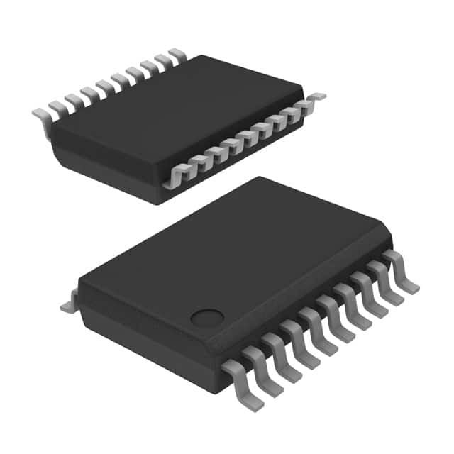
- Part No.:
- UPD78F9224MC-5A4-A
- Manufacturer:
- Renesas
- Category:
- Microcontrollers
- Package:
- -
- Datasheet:
-
 UPD78F9224MC-5A4-A.pdf
- Description:
- IC MCU
- Quantity:
- Payment:

- Shipping:

Inventory:1,916
Please send an inquiry. Send us your inquiry, and we will respond immediately.
Product details
Overview
UPD78F9224MC-5A4-A from Renesas Electronics is a 16-pin interface adapter that converts the 14-pin E1 emulator interface to the 16-pin interface used by QB-MINI2 and PG-FP5 programmers. It supports clock frequencies of 4/8/16 MHz, includes configurable jumpers (JP1–JP3) for UART programming and debug mode selection, and is designed for use with 78K0-series microcontrollers including uPD78F0711/0712/0714.
For engineers reviewing the UPD78F9224MC-5A4-A datasheet, UPD78F9224MC-5A4-A pinout, UPD78F9224MC-5A4-A application, or UPD78F9224MC-5A4-A equivalent, this adapter enables seamless transition between Renesas E1 emulation hardware and newer 16-pin programming tools while maintaining signal integrity and mode-specific routing for flash programming and debugging workflows.
Technical Context
The UPD78F9224MC-5A4-A implements passive pin mapping between two standardized Renesas debug interfaces: it routes E1's 14-pin signals-including TRST, TCK, TMS, TDI, TDO, RESET, VDD, GND, and clock outputs-to corresponding pins on the 16-pin QB-MINI2/PG-FP5 header. Signal translation requires no active logic or level shifting.
Jumper JP2 controls UART path isolation during debugging versus programming; JP3 enables/disables specific reset and programming signal routing for 78K0/Kx1+ devices; JP1 provides optional VDD sourcing configuration. All jumpers are solder-pad type requiring physical modification for reconfiguration.
Key Specifications
| Parameter | Value and Actual Design Meaning |
|---|---|
| Interface Conversion | 14-pin E1 emulator ↔ 16-pin QB-MINI2/PG-FP5 |
| Supported Clock Frequencies | 4 MHz, 8 MHz, and 16 MHz only - no other frequencies supported |
| Jumper Configuration | JP2: UART path isolation control; JP3: 78K0/Kx1+ reset/programming signal routing; JP1: VDD source selection |
| Target MCU Families | 78K0, 78K0/Kx1+, uPD78F0711, uPD78F0712, uPD78F0714 |
| Physical Construction | PCB-based passive adapter with solder-pad jumpers and fixed pin mapping |
Availability
UPD78F9224MC-5A4-A is available at Aetrix Electronics and suitable for embedded firmware development, production flash programming, and debug infrastructure deployment requiring stable component supply across Renesas 78K0-based design cycles.
Supply support for UPD78F9224MC-5A4-A includes scheduled delivery planning, volume procurement assistance, BOM continuity management, traceable sourcing, and lifecycle availability coordination for OEM customers, industrial embedded developers, connected-device designers, and electronics production programs.
Manufacturer
Renesas Electronics is a Japanese semiconductor manufacturer specializing in microcontrollers, analog, power, and SoC solutions for automotive, industrial, and IoT applications.
The UPD78F9224MC-5A4-A belongs to Renesas' legacy debug interface adapter product line, developed to extend compatibility between aging E1 emulators and next-generation 16-pin programming tools for 78K0-family MCUs.
FAQ
What is the primary function of the UPD78F9224MC-5A4-A?
The UPD78F9224MC-5A4-A is a passive PCB adapter that converts the 14-pin E1 emulator interface to the 16-pin interface used by QB-MINI2 and PG-FP5 programmers. It enables Renesas 78K0-family MCU development by bridging legacy and modern debug hardware without signal conditioning or active components.
Which microcontroller families are compatible with UPD78F9224MC-5A4-A?
The UPD78F9224MC-5A4-A is explicitly validated for use with 78K0, 78K0/Kx1+, uPD78F0711, uPD78F0712, and uPD78F0714 microcontrollers. Compatibility is defined by jumper configurations (JP2/JP3) and clock frequency support - no broader 78K family coverage is documented.
How do JP2 and JP3 affect UPD78F9224MC-5A4-A operation?
JP2 isolates the UART programming path during debugging to prevent conflicts when external UART devices are connected; JP3 modifies reset and programming signal routing specifically for 78K0/Kx1+ devices. Both require physical solder-pad modification - open for programming, shorted (default) for debugging per Renesas documentation.
Does UPD78F9224MC-5A4-A support clock frequencies other than 4/8/16 MHz?
No. The UPD78F9224MC-5A4-A relies on E1 emulator clock output, which is limited to 4 MHz, 8 MHz, and 16 MHz only. No circuitry or configuration within the UPD78F9224MC-5A4-A enables other frequencies - attempting to use unsupported clocks will result in failed communication or unstable debug sessions.
Is UPD78F9224MC-5A4-A a standalone programmer or an interface adapter?
The UPD78F9224MC-5A4-A is strictly a passive interface adapter - it contains no firmware, memory, or programmable logic. It performs only pin-to-pin signal routing between E1 and 16-pin headers. Programming and debugging functions remain fully handled by the connected E1 emulator, QB-MINI2, or PG-FP5 tool.
UPD78F9224MC-5A4-A Specifications
- Product attributes
- Attribute value
- Manufacturer:
- Renesas
- Package/Case:
- -
- Series:
- -
- Packaging:
- Tray
- Product Status:
- Obsolete
- Programmable:
- Not Verified
- Core Processor:
- -
- Core Size:
- -
- Speed:
- -
- Connectivity:
- -
- Peripherals:
- -
- Number of I/O:
- -
- Program Memory Size:
- -
- Program Memory Type:
- -
- EEPROM Size:
- -
- RAM Size:
- -
- Voltage - Supply (Vcc/Vdd):
- -
- Data Converters:
- -
- Oscillator Type:
- -
- Operating Temperature:
- -
- Grade:
- -
- Qualification:
- -
- Mounting Type:
- -
- Supplier Device Package:
UPD78F9224MC-5A4-A FAQ
1.How can I place an order for UPD78F9224MC-5A4-A through Aetrix?
Please submit a Request for Quotation (RFQ) for UPD78F9224MC-5A4-A on Aetrix. Our sales agent will provide a competitive quotation and guide you through the order confirmation once you accept the terms.
2.Are the price and stock information for UPD78F9224MC-5A4-A reliable?
The price and inventory of UPD78F9224MC-5A4-A are updated periodically and may fluctuate due to market conditions. Stock and pricing data are typically refreshed every 24 hours. Quotation validity for UPD78F9224MC-5A4-A is usually 5 days.
3.What payment methods are accepted for UPD78F9224MC-5A4-A?
We accept Wire Transfer, PayPal, Credit Card, Western Union, MoneyGram, and Escrow for UPD78F9224MC-5A4-A transactions.
Note: Certain payment methods may incur a processing fee.
4.How is shipping managed for UPD78F9224MC-5A4-A?
UPD78F9224MC-5A4-A orders can be shipped via leading logistics carriers, including DHL, UPS, FedEx, TNT, or Registered Mail.
Once your UPD78F9224MC-5A4-A order is processed, you will receive an email with the shipment details and tracking number.
Note: Tracking information may take up to 24 hours to appear. Express delivery typically takes 3–5 business days.
5.How can I obtain technical support or documentation for UPD78F9224MC-5A4-A?
For technical support, including UPD78F9224MC-5A4-A datasheets, pinout diagrams, or application guidance, please contact our engineering support team. They can provide detailed documentation and assistance for your UPD78F9224MC-5A4-A requirements.
6.How does Aetrix verify that UPD78F9224MC-5A4-A is sourced from the original manufacturer or authorized distributors?
All UPD78F9224MC-5A4-A products on Aetrix are procured from qualified distributors and authorized channels. Our dedicated quality assurance team conducts strict verification, including traceability checks and, if necessary, third-party testing. This ensures that UPD78F9224MC-5A4-A meets industry standards.
7.What is the process for return or replacement of UPD78F9224MC-5A4-A?
All UPD78F9224MC-5A4-A units undergo pre-shipment inspection (PSI). If there is an issue with UPD78F9224MC-5A4-A, returns or replacements are accepted under the following conditions:
1.Quantity discrepancies, incorrect items, or visible external defects (such as breakage or corrosion), acknowledged by Aetrix.
2.The issue is reported within 90 days of delivery.
3.The UPD78F9224MC-5A4-A part is unused and in its original packaging.
Return procedure for UPD78F9224MC-5A4-A:
1.Submit a request within 90 days.
2.Obtain a Return Material Authorization (RMA) from Aetrix.
UPD78F9224MC-5A4-A Tags

-
ATTINY4-TSHR
Microchip Technology
-
ATTINY10-TSHR
Microchip Technology
-
ATTINY10-TS8R
Microchip Technology

-
ATTINY202-SSNR
Microchip Technology
-
ATTINY202-SSFR
Microchip Technology
-
ATTINY402-SSNR
Microchip Technology

-
PIC16F15213T-I/MF
Microchip Technology
-
PIC16F15213-E/MF
Microchip Technology

-
PIC10F200T-I/OT
Microchip Technology
-
ATTINY412-SSNR
Microchip Technology
-
PIC10F202T-I/OT
Microchip Technology

-
ATTINY404-SSNR
Microchip Technology
Tech Hub

A practical engineering and sourcing framework covering lifecycle verification, lifetime-buy calculations, replacement qualification, supplier checks and counterfeit-risk controls.

TTL and CMOS logic families differ in thresholds, loading, output drive, power and timing. This engineering guide compares 74HC and 74HCT, calculates noise margins and checks 3.3 V/5 V compatibility.

A practical engineering guide to 3.3V and 5V logic compatibility, input thresholds, resistor dividers, translator ICs, MOSFET level shifting, I2C pull-ups, timing limits and power-sequencing risks.

The 74HC595 uses push-pull logic outputs, while the TPIC6B595 uses 50 V open-drain DMOS sinks for higher-power loads. This guide compares timing, current limits, 3.3 V interfacing, load wiring, thermal…

The 74HC595 converts serial data into eight stable parallel outputs. This guide covers pin functions, shift and storage timing, OE and MR behavior, drive-current limits, cascading, voltage compatibilit…

A technical comparison of level-sensitive latches and edge-triggered flip-flops, covering timing windows, setup and hold limits, master–slave operation, time borrowing, race-through, HDL inference and…

A D latch stores one bit while Enable controls when data can pass. This reference covers gate-level operation, truth tables, transparency, setup and hold timing, LE versus OE, common ICs and practical …

An SR latch stores one bit through cross-coupled feedback. This engineering reference covers NOR and NAND implementations, truth tables, forbidden-state recovery, gated operation, switch debouncing, fa…

Latch circuits retain one bit through feedback. This technical reference covers SR and D latches, truth tables, transparency, timing limits, latch-versus-flip-flop behavior, applications and common log…

An engineering guide to LED driver operation, constant-current and constant-voltage outputs, linear and switching topologies, dimming, IC selection, calculations, replacement compatibility, and fault c…


