
 My Inquiry
 My Account


Renesas UPD8880CY-A
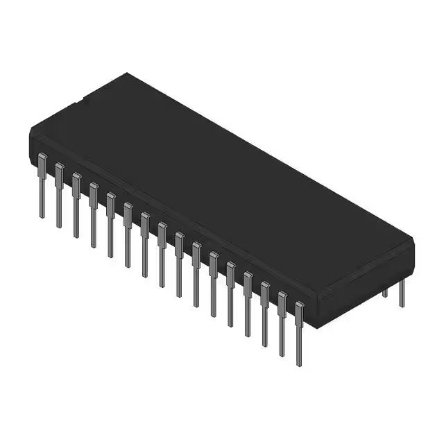
- Part No.:
- UPD8880CY-A
- Manufacturer:
- Renesas
- Category:
- Image Sensors, Camera
- Package:
- -
- Datasheet:
-
 UPD8880CY-A.pdf
- Description:
- CCD IMAGE SENSOR
- Quantity:
- Payment:

- Shipping:

Inventory:3,000
Please send an inquiry. Send us your inquiry, and we will respond immediately.
Product details
Overview
UPD8880CY-A from Renesas Electronics is a 3-color CCD linear image sensor with (10680+10680) × 3 staggered pixels, 4 µm photocell pitch, and dual-sided analog shift register readout architecture. It delivers 2400 dpi resolution for A4/US letter scanning, features on-chip reset feed-through level clamp circuits and voltage amplifiers, and operates at +12 V supply with CMOS-compatible 5 V drive clocks.
For engineers reviewing the UPD8880CY-A datasheet, UPD8880CY-A pinout, UPD8880CY-A application, or UPD8880CY-A equivalent, this page provides verified technical context for high-resolution color document scanning systems requiring stable analog output linearity, low image lag (<7%), and spectral response matched to red (630 nm), green (540 nm), and blue (460 nm) primary filters.
Technical Context
The UPD8880CY-A implements a triple-row, staggered photodiode array with separate red, green, and blue pixel lines spaced at 64 µm (16-line offset between R/G and G/B) and 8 µm (2-line offset within each color). Each row uses dual-sided charge transfer registers clocked by independent φ1/φ2 and φ1L/φ2L signals to achieve high-speed, low-noise readout.
It integrates on-chip signal conditioning: reset feed-through level clamp (driven by φCLB), voltage amplifiers per output channel (VOUT1–VOUT3), and internal bias generation for CCD transfer gates (φTG1–φTG3). Timing supports both bit-clamp and line-clamp modes, with data rate up to 8 MHz and total transfer efficiency ≥92% at 6 MHz clocking.
Key Specifications
| Parameter | Value and Actual Design Meaning |
|---|---|
| Resolution | 2400 dpi on US letter shorter side; enables high-fidelity A4 color scanning without interpolation |
| Photocell count | (10680+10680) × 3 valid pixels; supports full-width A4 (210 mm) capture at 96 dot/mm |
| Pixel pitch | 4 µm; determines optical sampling density and minimum resolvable feature size |
| Data rate | Up to 8 MHz; sets maximum line scan speed in high-throughput document scanners |
| Power supply | +12 V (11.4–12.6 V typical); requires stable low-noise rail for analog output stability |
| Dynamic range | DR1 ≥ 1750× (Vsat1/DSNU); ensures usable contrast across varying illumination in office environments |
| Image lag | 1.0–7.0%; directly impacts motion artifact suppression in fast-moving paper feed systems |
| Response peak | Red: 630 nm, Green: 540 nm, Blue: 460 nm; matches pigment-based RGB filter spectral transmission |
Pinout & Package
UPD8880CY-A is housed in a 32-pin plastic DIP package (10.16 mm width, 55.2 mm length) with integrated optical plastic cap. Pins marked "IC" (6, 7, 11, 12, 21, 22, 26, 27) must remain unconnected; NC pins (1, 8, 9, 10, 23, 24, 25, 28, 29, 30) require connection to GND.
| Pin/Terminal | Circuit Role | Design Meaning |
|---|---|---|
| 1, 8, 9, 10, 23, 24, 25, 28, 29, 30 | No connection (NC) | Must be tied to GND to prevent floating noise coupling into analog outputs |
| 2 | Reset gate clock (φRB) | Controls charge reset timing; high-level active during clamp period |
| 3 | Reset feed-through level clamp clock (φCLB) | Enables correlated double sampling; inverse of φTG1–φTG3 usable as alternative |
| 4, 13 | Shift register clock 1 (φ1) | Dual-pin input for balanced drive; total capacitance 2200 pF limits max trace length |
| 5, 20 | Shift register clock 2 (φ2) | Dual-pin input synchronized with φ1; cross-point timing critical for charge transfer integrity |
| 14 | Last stage shift register clock 1 (φ1L) | Drives final stage of analog shift register; low 70 pF capacitance eases driver design |
| 19 | Last stage shift register clock 2 (φ2L) | Complements φ1L for dual-sided readout; timing alignment prevents line skew |
| 15, 17, 18 | Transfer gate clocks (φTG3, φTG2, φTG1) | Control color-specific charge transfer; staggered activation enables RGB interleaving |
| 31, 32, 16 | Output signals (VOUT1-Blue, VOUT2-Green, VOUT3-Red) | Analog voltage outputs; 0.3–1 kΩ impedance requires 50 Ω termination for clean scope measurement |
| 31 | VOUT1 (Blue) | Valid pixel output for blue-filtered row; DC offset 4.5–7.5 V requires AC-coupling or level-shifting |
| 32 | VOUT2 (Green) | Valid pixel output for green-filtered row; same offset range and noise floor as VOUT1/VOUT3 |
| 16 | VOUT3 (Red) | Valid pixel output for red-filtered row; lower responsivity (1.26–2.34 V/lx·s) vs. green/blue |
| 22 | VOD | Output drain voltage supply; +12 V input powers on-chip amplifiers and clamp circuits |
| 7, 12, 21, 26, 27 | Internal connection (IC) | Internally bonded; must remain open-no external connection permitted |
Key Features
| Feature | Design Value |
|---|---|
| Triple-color staggered pixel array | Enables simultaneous RGB line capture without mechanical filter wheel, reducing scan time and complexity |
| Dual-sided analog shift register | Halves effective readout time per line versus single-sided architecture, supporting >8 MHz data rates |
| On-chip reset feed-through level clamp | Provides correlated double sampling (CDS) to suppress reset noise (RFTN: −2000 to +500 mV) |
| Pigment-based primary color filter | Light resistance ≥10⁷ lx·hour ensures long-term spectral stability in high-intensity scanner lamps |
| CMOS-compatible 5 V drive clocks | Allows direct interface with standard logic families (74AC04/74HC04) without level-shifting circuitry |
| Optical black reference pixels | 48-pixel black reference per line enables real-time DC offset calibration and temperature drift compensation |
Applications
| High-Resolution Document Scanning | Color Facsimile Transmission |
|---|---|
Use Scenario: A4-size color document digitization in enterprise multifunction printers with 2400 dpi optical resolution requirement. IC Role / Device Role / Timing Role: Primary image capture device; provides three synchronized analog RGB outputs per scan line with sub-millisecond timing precision. Use Value: Eliminates need for mechanical color filter sequencing, enabling single-pass full-color capture at production-grade speeds. |
Use Scenario: High-fidelity color fax transmission compliant with ITU-T T.4/T.6 standards for legal and medical records. IC Role / Device Role / Timing Role: Line-scan sensor feeding JPEG-compressed RGB data to modem subsystem; timing locked to line sync generator. Use Value: 64 µm line spacing and 4 µm pitch ensure accurate reproduction of fine text and halftone patterns without aliasing. |
| Flatbed Scanner Imaging Engine | Industrial Barcode Verification System |
Use Scenario: OEM flatbed scanner module requiring low-power, high-SNR analog front-end for reflective media. IC Role / Device Role / Timing Role: Analog imaging core; outputs calibrated RGB voltages to external ADC with programmable gain control. Use Value: On-chip voltage amplifiers and level clamping reduce BOM count and PCB area versus discrete op-amp solutions. |
Use Scenario: High-speed verification of 2D matrix barcodes (PDF417, Data Matrix) printed on packaging with variable contrast. IC Role / Device Role / Timing Role: Precision line sensor capturing spectral reflectance across red/green/blue bands to validate ink density and registration. Use Value: Spectral response peaks at 630/540/460 nm enable discrimination of cyan/magenta/yellow inks via RGB ratio analysis. |
Equivalent & Alternatives
The following parts are listed as comparable options for similar CCD linear image sensor applications.
| Alternative Part | Technical Difference | Application Difference | Selection Advice |
|---|---|---|---|
| TCD2252D | Single-channel monochrome output; 5000-pixel array; no on-chip clamp or amplifiers; requires external CDS and gain stages | Suitable only for grayscale scanning; lacks RGB separation and integrated signal conditioning | Select when cost sensitivity outweighs color fidelity and system integration needs |
| ILX521A | 2048-pixel tri-linear array; 14 µm pitch; separate RGB outputs; no on-chip clamp; higher dark current (ADS up to 12 mV) | Lower resolution and coarser pitch limit use to medium-duty scanners; greater thermal drift affects long-run stability | Prefer for compact form factor where 2400 dpi is not mandatory and thermal management is constrained |
Compared with TCD2252D and ILX521A, the UPD8880CY-A provides full-color capture in a single device with integrated clamping and amplification, enabling simpler, higher-performance scanner designs-but requires more complex clock sequencing and tighter power supply regulation.
Availability
UPD8880CY-A is available at Aetrix Electronics and suitable for high-resolution document scanning, color facsimile transmission, and industrial barcode verification requiring stable component supply and long-lifecycle support.
Supply support for UPD8880CY-A includes scheduled delivery planning, volume procurement assistance, BOM continuity management, traceable sourcing, and lifecycle availability coordination for OEM customers, industrial embedded developers, connected-device designers, and electronics production programs.
Manufacturer
Renesas Electronics Corporation is a global semiconductor leader specializing in microcontrollers, analog, power, and sensor solutions for industrial, automotive, and infrastructure markets.
The UPD8880CY-A belongs to Renesas' legacy CCD linear image sensor product line, designed specifically for high-accuracy, high-speed color document capture in office and industrial imaging equipment.
FAQ
What is the maximum recommended data rate for UPD8880CY-A in bit-clamp mode?
The UPD8880CY-A supports a maximum data rate of 8 MHz in bit-clamp mode, as specified in the Recommended Operating Conditions table. At this rate, saturation voltage Vsat1 remains ≥2.5 V and image lag stays within 7.0%, provided fφ1/fφ2 ≤ 6 MHz and VOD is maintained at 12.0 V ±0.6 V. Exceeding 8 MHz risks increased image lag and reduced dynamic range due to incomplete charge transfer.
How should unused IC pins be handled on the UPD8880CY-A?
Unused IC pins (6, 7, 11, 12, 21, 22, 26, 27) on the UPD8880CY-A must remain unconnected-no pull-up, pull-down, or grounding is permitted. These pins are internally bonded to substrate or bias networks; external connection may disrupt internal voltage references or cause latch-up. The datasheet explicitly cautions against any connection to these terminals.
Does UPD8880CY-A include optical black reference pixels, and how are they used?
Yes, the UPD8880CY-A includes 48 optical black reference pixels per color line, located at the end of each valid pixel segment. These shielded pixels provide real-time DC offset and thermal drift compensation: their output is sampled during the blanking interval and subtracted from active pixel data via external CDS circuitry or digital post-processing, improving PRNU and DSNU performance.
What is the significance of the 64 µm line spacing specification for UPD8880CY-A?
The 64 µm line spacing between red-green and green-blue rows in the UPD8880CY-A enables precise vertical color registration in single-pass scanning. Combined with 8 µm intra-color line spacing, it allows reconstruction of full RGB samples per physical scan line without interpolation-critical for avoiding color fringing in high-resolution text and graphics reproduction.
Can UPD8880CY-A operate with a 3.3 V logic interface for clock inputs?
No, UPD8880CY-A requires CMOS-level clock inputs referenced to its +12 V supply: shift register clocks (φ1/φ2) demand 4.8–5.5 V high level and −0.3–0.2 V low level. A 3.3 V logic interface would fall below the VIH(min) threshold, causing unreliable clock edge detection and potential charge transfer failure. Level-shifting to 5 V is mandatory.
UPD8880CY-A Specifications
- Product attributes
- Attribute value
- Manufacturer:
- Renesas
- Series:
- *
- Package/Case:
- -
- Packaging:
- Bulk
- Product Status:
- Active
- Type:
- -
- Pixel Size:
- -
- Active Pixel Array:
- -
- Frames per Second:
- -
- Voltage - Supply:
- -
- Supplier Device Package:
- -
- Operating Temperature:
- -
- Grade:
- -
- Qualification:
- -
UPD8880CY-A FAQ
1.How can I place an order for UPD8880CY-A through Aetrix?
Please submit a Request for Quotation (RFQ) for UPD8880CY-A on Aetrix. Our sales agent will provide a competitive quotation and guide you through the order confirmation once you accept the terms.
2.Are the price and stock information for UPD8880CY-A reliable?
The price and inventory of UPD8880CY-A are updated periodically and may fluctuate due to market conditions. Stock and pricing data are typically refreshed every 24 hours. Quotation validity for UPD8880CY-A is usually 5 days.
3.What payment methods are accepted for UPD8880CY-A?
We accept Wire Transfer, PayPal, Credit Card, Western Union, MoneyGram, and Escrow for UPD8880CY-A transactions.
Note: Certain payment methods may incur a processing fee.
4.How is shipping managed for UPD8880CY-A?
UPD8880CY-A orders can be shipped via leading logistics carriers, including DHL, UPS, FedEx, TNT, or Registered Mail.
Once your UPD8880CY-A order is processed, you will receive an email with the shipment details and tracking number.
Note: Tracking information may take up to 24 hours to appear. Express delivery typically takes 3–5 business days.
5.How can I obtain technical support or documentation for UPD8880CY-A?
For technical support, including UPD8880CY-A datasheets, pinout diagrams, or application guidance, please contact our engineering support team. They can provide detailed documentation and assistance for your UPD8880CY-A requirements.
6.How does Aetrix verify that UPD8880CY-A is sourced from the original manufacturer or authorized distributors?
All UPD8880CY-A products on Aetrix are procured from qualified distributors and authorized channels. Our dedicated quality assurance team conducts strict verification, including traceability checks and, if necessary, third-party testing. This ensures that UPD8880CY-A meets industry standards.
7.What is the process for return or replacement of UPD8880CY-A?
All UPD8880CY-A units undergo pre-shipment inspection (PSI). If there is an issue with UPD8880CY-A, returns or replacements are accepted under the following conditions:
1.Quantity discrepancies, incorrect items, or visible external defects (such as breakage or corrosion), acknowledged by Aetrix.
2.The issue is reported within 90 days of delivery.
3.The UPD8880CY-A part is unused and in its original packaging.
Return procedure for UPD8880CY-A:
1.Submit a request within 90 days.
2.Obtain a Return Material Authorization (RMA) from Aetrix.
UPD8880CY-A Tags

-
MT9M114EBLSTCZ-CR
onsemi
-
EPC611-CSP24-001
ESPROS Photonics AG
-
AR0147ATSC00XUEG5-DRBR
onsemi
-
AR0130CSSM00SPCA0-DRBR
onsemi
-
AR1335CSSC11SMKA0-CP
onsemi
-
AR0521SR2M09SURA0-DP
onsemi
-
AR0135CS2M25SUEA0-DPBR
onsemi
-
AR0522SRSC09SURA0-DP
onsemi
-
AR0134CSSC00SPCA0-DPBR
onsemi
-
AR0134CSSM00SUEA0-DPBR
onsemi
-
AR0521SR2C09SURA0-DP
onsemi
-
AR0135CS2M00SUEA0-DPBR
onsemi
Tech Hub

TTL and CMOS logic families differ in thresholds, loading, output drive, power and timing. This engineering guide compares 74HC and 74HCT, calculates noise margins and checks 3.3 V/5 V compatibility.

A practical engineering guide to 3.3V and 5V logic compatibility, input thresholds, resistor dividers, translator ICs, MOSFET level shifting, I2C pull-ups, timing limits and power-sequencing risks.

The 74HC595 uses push-pull logic outputs, while the TPIC6B595 uses 50 V open-drain DMOS sinks for higher-power loads. This guide compares timing, current limits, 3.3 V interfacing, load wiring, thermal…

The 74HC595 converts serial data into eight stable parallel outputs. This guide covers pin functions, shift and storage timing, OE and MR behavior, drive-current limits, cascading, voltage compatibilit…

A technical comparison of level-sensitive latches and edge-triggered flip-flops, covering timing windows, setup and hold limits, master–slave operation, time borrowing, race-through, HDL inference and…

A D latch stores one bit while Enable controls when data can pass. This reference covers gate-level operation, truth tables, transparency, setup and hold timing, LE versus OE, common ICs and practical …

An SR latch stores one bit through cross-coupled feedback. This engineering reference covers NOR and NAND implementations, truth tables, forbidden-state recovery, gated operation, switch debouncing, fa…

Latch circuits retain one bit through feedback. This technical reference covers SR and D latches, truth tables, transparency, timing limits, latch-versus-flip-flop behavior, applications and common log…

An engineering guide to LED driver operation, constant-current and constant-voltage outputs, linear and switching topologies, dimming, IC selection, calculations, replacement compatibility, and fault c…

Operational amplifier guide covering op amp basics, feedback, ideal vs real op amps, common configurations, buffer circuits, offset, bias current, gain-bandwidth, slew rate, rail-to-rail limits and sel…


