
 My Inquiry
 My Account


Microchip Technology USB2660I-JZX-03
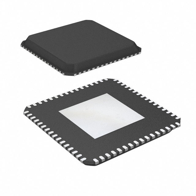
- Part No.:
- USB2660I-JZX-03
- Manufacturer:
- Microchip Technology
- Category:
- Specialized
- Package:
- 64-VFQFN Exposed Pad
- Datasheet:
-
 USB2660I-JZX-03.pdf
- Description:
- IC INTERFACE SPECIALIZED 64QFN
- Quantity:
- Payment:

- Shipping:

Inventory:400
Please send an inquiry. Send us your inquiry, and we will respond immediately.
Product details
Overview
USB2660I-JZX-03 from Microchip (formerly SMSC) is an industrial-grade, single-chip USB 2.0 Hi-Speed hub and multi-format flash media controller with dual SD interfaces. It integrates a 2-port downstream USB hub, transaction translator (TT), 8051 microprocessor (60 MHz), 64 KB ROM / 9 KB RAM, and dual SD/SDIO controllers supporting SD 2.0, MMC 4.2, Memory Stick 1.43, MS-Pro 1.02, MS-Duo 1.10, and xD-Picture Card 1.2 - used in GPS navigation systems and industrial media players for simultaneous card read/write and peripheral expansion.
For engineers reviewing the USB2660I-JZX-03 datasheet, USB2660I-JZX-03 pinout, USB2660I-JZX-03 application, or USB2660I-JZX-03 equivalent, key selection criteria include industrial temperature range (-40°C to +85°C), dual SD interface capability (one multiplexed, one dedicated SDIO), PHYBoost signal integrity tuning, PortSwap differential-pair remapping, and support for external SPI/I²C configuration ROMs.
Technical Context
The USB2660I-JZX-03 implements a fully compliant USB 2.0 hub with integrated TT for concurrent Low-Speed, Full-Speed, and Hi-Speed downstream device operation. Its flash media subsystem includes two independent SD controllers: one multiplexed interface handling SD/MMC/MS/xD via shared pins, and a second non-multiplexed SD/SDIO slot enabling wireless co-location (e.g., Wi-Fi/Bluetooth modules).
It features programmable hardware blocks including PortMap (dynamic port disable/reordering), PortSwap (per-port D+/D− pin assignment), and PHYBoost (four-level transceiver drive strength). Configuration is loaded at boot from external I²C EEPROM or SPI Flash, supporting customizable VID/PID, device strings, and GPIO mapping.
Key Specifications
| Parameter | Value and Actual Design Meaning |
|---|---|
| USB Compliance | USB 2.0 Hi-Speed hub with TT; supports LS/FS/HS devices on all enabled ports |
| Flash Media Support | SD 2.0 / MMC 4.2 / MS 1.43 / MS-Pro 1.02 / MS-Duo 1.10 / xD 1.2 - verified per spec |
| Operating Temp | -40°C to +85°C - qualified for industrial embedded applications |
| Memory Resources | 64 KB on-chip ROM + 9 KB RAM - sufficient for firmware execution and media protocol stacks |
| Supply & Regulation | Single 3.3 V input; internal 1.8 V core regulator reduces BOM count and power loss |
| GPIO Count | Up to 20 configurable GPIOs - includes two 200 mA drive outputs with fold-back short-circuit protection |
| Package | 64-pin QFN (9 × 9 mm, RoHS/halogen-free) - surface-mount compatible with standard reflow profiles |
Pinout & Package
USB2660I-JZX-03 is housed in a 64-pin QFN package (9 mm × 9 mm, 0.5 mm pitch) with exposed thermal pad connected to VSS. Pin functions are validated per SMSC datasheet Rev. 1.1 (2010), Table 6.1 and Figure 3.1.
| Pin/Terminal | Circuit Role | Design Meaning |
|---|---|---|
| USBDN_DP2 / USBDN_DM2 | Downstream USB Port 2 differential pair | Hi-Speed-capable D+/D− signals for external peripheral connection; supports PHYBoost tuning |
| USBDN_DP3 / USBDN_DM3 | Downstream USB Port 3 differential pair | Internal connection to flash media reader as Compound Device; not exposed externally |
| SD1_CLK / SD2_CLK | SD interface clock outputs | Configurable clock rates up to 50 MHz for SD/SDIO; supports SDR/DDR modes per spec |
| SD1_D0–D7 / SD2_D0–D7 | SD data bus terminals | Dual 8-bit bidirectional data paths - SD1 supports multiplexed formats; SD2 is dedicated SD/SDIO |
| GPIO6 / GPIO15–19 | Configurable general-purpose I/O | Programmable direction, pull-up/down, and interrupt capability; two pins support 200 mA sink/source |
Key Features
| Feature | Design Value |
|---|---|
| Dual SD Interface Architecture | One multiplexed SD/MMC/MS/xD interface + one dedicated SD/SDIO slot enables simultaneous card access and wireless bridging (e.g., Wi-Fi + SD) |
| PHYBoost Signal Integrity | Four programmable USB transceiver drive levels restore eye diagram margin in electrically noisy or long-trace PCB layouts |
| PortSwap Pin Remapping | Per-port D+/D− pin assignment eliminates trace crossing and unequal length routing - simplifies 2-layer board design |
| PortMap Dynamic Reordering | Automatic downstream port renumbering after disable maintains host OS compatibility without firmware changes |
| Flexible Boot Configuration | Supports I²C EEPROM or SPI Flash for vendor ID, product ID, serial number, and GPIO mapping - no mask ROM required |
Applications
| GPS Navigation Systems | Industrial Media Players |
|---|---|
Use Scenario: Embedded vehicle navigation unit with SD card map storage and USB peripheral connectivity (e.g., cellular dongle, printer). IC Role / Device Role / Timing Role: USB2660I-JZX-03 acts as compound hub + SD controller - managing upstream host link, two downstream USB ports, and dual SD slots for map updates and logging. Use Value: Enables concurrent SD card read/write and USB peripheral operation without CPU intervention; industrial temp rating ensures reliability in automotive cabin environments. | Use Scenario: Ruggedized media player for factory floor displays, supporting SD-based firmware updates and USB-connected barcode scanners. IC Role / Device Role / Timing Role: USB2660I-JZX-03 serves as hub controller and flash media interface - providing isolated power control per port and deterministic SD transfer timing via dedicated SDIO lane. Use Value: Dual SD interfaces allow hot-swap firmware update (SD1) while streaming video from SD2; ganged port power control simplifies industrial power sequencing. |
| Set-Top Boxes | Printers with Card Readers |
Use Scenario: Consumer set-top box with SD card content import, USB storage expansion, and optional Bluetooth audio adapter. IC Role / Device Role / Timing Role: USB2660I-JZX-03 operates as Hi-Speed hub with integrated SDIO bridge - connecting SD card, USB HDD, and Bluetooth module via single USB upstream link. Use Value: SDIO bridging over Port 3 enables low-latency wireless coexistence; PHYBoost compensates for signal degradation across dense PCB layouts. | Use Scenario: Multifunction office printer with built-in SD card reader, USB host for flash drives, and optional NFC module via SDIO. IC Role / Device Role / Timing Role: USB2660I-JZX-03 functions as compound device - exposing SD reader as USB mass storage while managing USB peripheral enumeration and SDIO command flow. Use Value: Eliminates need for separate SD controller IC; configurable GPIOs drive status LEDs and detect card insertion/removal events. |
Equivalent & Alternatives
The following parts are listed as comparable options for similar USB hub + flash media controller applications.
| Alternative Part | Technical Difference | Application Difference | Selection Advice |
|---|---|---|---|
| USB2640I-JZX | 4-port hub (vs. 2-port); no dual SD interfaces - single SD/SDIO only; same industrial temp range | Lacks multiplexed flash format support (MS/xD); unsuitable for legacy card compatibility requirements | Select when higher USB port count is prioritized over multi-format SD flexibility |
| USB5744-ABZ | 4-port USB 2.0 hub only - no integrated flash media controller; requires external SDIO host controller | Cannot replace USB2660I-JZX-03's dual SD functionality; adds BOM cost and layout complexity | Choose only if flash media is handled separately and hub port density is critical |
Compared with USB2640I-JZX and USB5744-ABZ, the USB2660I-JZX-03 uniquely delivers dual SD interfaces (multiplexed + dedicated SDIO) within a 2-port industrial hub - reducing component count and enabling SDIO wireless co-location without external logic.
Availability
USB2660I-JZX-03 is available at Aetrix Electronics and suitable for GPS navigation systems, industrial media players, set-top boxes, and printers requiring stable component supply, long-term lifecycle support, and industrial temperature qualification.
Supply support for USB2660I-JZX-03 includes scheduled delivery planning, volume procurement assistance, BOM continuity management, traceable sourcing, and lifecycle availability coordination for OEM customers, industrial embedded developers, connected-device designers, and electronics production programs.
Manufacturer
Microchip Technology acquired SMSC in 2012 and maintains full support for legacy SMSC USB hub and interface ICs. The company specializes in embedded control and connectivity solutions.
The USB2660I-JZX-03 belongs to SMSC's Ultra Fast USB Hub + Flash Media Controller product line, designed specifically for cost-sensitive, space-constrained industrial and consumer devices requiring integrated USB expansion and multi-format SD/SDIO support.
FAQ
What is the operating temperature range of the USB2660I-JZX-03?
The USB2660I-JZX-03 is rated for industrial operation from -40°C to +85°C. This specification is explicitly defined in the SMSC datasheet Rev. 1.1 (Section 8.1.2) and distinguishes it from the commercial-grade USB2660 variant (0°C to +70°C). The extended range makes USB2660I-JZX-03 suitable for deployment in uncontrolled environments such as vehicle cabins, factory floors, and outdoor kiosks where ambient temperatures exceed commercial limits.
Does the USB2660I-JZX-03 support xD-Picture Card, and what licensing is required?
Yes, the USB2660I-JZX-03 supports xD-Picture Card 1.2 per its datasheet (Section "Compliance"). However, SMSC mandates that end customers obtain a separate license from Fuji Photo Film Co., Ltd., Olympus Optical Co., Ltd., and Toshiba Corporation prior to use. Purchasing USB2660I-JZX-03 does not confer xD rights; SMSC reserves the right to discontinue supply if licensing is not maintained. This requirement applies exclusively to USB2660I-JZX-03 units configured for xD operation.
How many SD interfaces does the USB2660I-JZX-03 provide, and how are they implemented?
The USB2660I-JZX-03 provides two physically distinct SD interfaces: one multiplexed interface (SD1) supporting SD/MMC/MS/xD via shared pins, and one dedicated non-multiplexed SD/SDIO interface (SD2) intended for SDIO bridging (e.g., Wi-Fi, Bluetooth). Both are independently clocked and controlled. SD1 uses pin-sharing per Table 6.1; SD2 has dedicated D0–D7, CLK, CMD, and nCD/WP lines - confirmed in Section 1 Overview and Pin Descriptions.
Can the USB2660I-JZX-03 be configured without external memory?
No - the USB2660I-JZX-03 requires external configuration memory. It boots from either an I²C EEPROM or SPI Flash device containing VID/PID, device descriptors, GPIO mapping, and port configuration. There is no internal mask-ROM option; the "default configuration" referenced in Section 8.5 is minimal and non-functional for production use. External ROM is mandatory for USB enumeration and flash media initialization.
What is the purpose of the PortSwap feature in the USB2660I-JZX-03?
PortSwap allows per-port reassignment of USB differential pair (D+/D−) pin locations on the USB2660I-JZX-03's 64-pin QFN package. This enables direct alignment of D+/D− traces to USB connectors without crossing or length mismatch - critical for maintaining Hi-Speed signal integrity on compact or 2-layer PCBs. PortSwap is configured via internal registers during initialization and does not require hardware modification.
USB2660I-JZX-03 Specifications
- Product attributes
- Attribute value
- Manufacturer:
- Microchip Technology
- Series:
- -
- Package/Case:
- 64-VFQFN Exposed Pad
- Packaging:
- Tray
- Product Status:
- Active
- Applications:
- Desktop, Notebook PCs
- Interface:
- -
- Voltage - Supply:
- -
- Supplier Device Package:
- 64-QFN (9x9)
- Grade:
- -
- Qualification:
- -
- Mounting Type:
- Surface Mount
USB2660I-JZX-03 FAQ
1.How can I place an order for USB2660I-JZX-03 through Aetrix?
Please submit a Request for Quotation (RFQ) for USB2660I-JZX-03 on Aetrix. Our sales agent will provide a competitive quotation and guide you through the order confirmation once you accept the terms.
2.Are the price and stock information for USB2660I-JZX-03 reliable?
The price and inventory of USB2660I-JZX-03 are updated periodically and may fluctuate due to market conditions. Stock and pricing data are typically refreshed every 24 hours. Quotation validity for USB2660I-JZX-03 is usually 5 days.
3.What payment methods are accepted for USB2660I-JZX-03?
We accept Wire Transfer, PayPal, Credit Card, Western Union, MoneyGram, and Escrow for USB2660I-JZX-03 transactions.
Note: Certain payment methods may incur a processing fee.
4.How is shipping managed for USB2660I-JZX-03?
USB2660I-JZX-03 orders can be shipped via leading logistics carriers, including DHL, UPS, FedEx, TNT, or Registered Mail.
Once your USB2660I-JZX-03 order is processed, you will receive an email with the shipment details and tracking number.
Note: Tracking information may take up to 24 hours to appear. Express delivery typically takes 3–5 business days.
5.How can I obtain technical support or documentation for USB2660I-JZX-03?
For technical support, including USB2660I-JZX-03 datasheets, pinout diagrams, or application guidance, please contact our engineering support team. They can provide detailed documentation and assistance for your USB2660I-JZX-03 requirements.
6.How does Aetrix verify that USB2660I-JZX-03 is sourced from the original manufacturer or authorized distributors?
All USB2660I-JZX-03 products on Aetrix are procured from qualified distributors and authorized channels. Our dedicated quality assurance team conducts strict verification, including traceability checks and, if necessary, third-party testing. This ensures that USB2660I-JZX-03 meets industry standards.
7.What is the process for return or replacement of USB2660I-JZX-03?
All USB2660I-JZX-03 units undergo pre-shipment inspection (PSI). If there is an issue with USB2660I-JZX-03, returns or replacements are accepted under the following conditions:
1.Quantity discrepancies, incorrect items, or visible external defects (such as breakage or corrosion), acknowledged by Aetrix.
2.The issue is reported within 90 days of delivery.
3.The USB2660I-JZX-03 part is unused and in its original packaging.
Return procedure for USB2660I-JZX-03:
1.Submit a request within 90 days.
2.Obtain a Return Material Authorization (RMA) from Aetrix.
USB2660I-JZX-03 Tags

-
NVT4857UKAZ
NXP Semiconductors

-
TCA8418RTWR
Texas Instruments

-
PCA9546APWR
Texas Instruments

-
MD0100N8-G
Microchip Technology

-
PCA9548APW,118
NXP Semiconductors

-
PCA9540BDP,118
NXP Semiconductors

-
PCA9548APWR
Texas Instruments

-
PCA9546APW,118
NXP Semiconductors

-
PTN3360DBS,518
NXP Semiconductors

-
PCA9546ABS,118
NXP Semiconductors

-
PCA9518PWR
Texas Instruments

-
PCA9545APW,118
NXP Semiconductors
Tech Hub

TTL and CMOS logic families differ in thresholds, loading, output drive, power and timing. This engineering guide compares 74HC and 74HCT, calculates noise margins and checks 3.3 V/5 V compatibility.

A practical engineering guide to 3.3V and 5V logic compatibility, input thresholds, resistor dividers, translator ICs, MOSFET level shifting, I2C pull-ups, timing limits and power-sequencing risks.

The 74HC595 uses push-pull logic outputs, while the TPIC6B595 uses 50 V open-drain DMOS sinks for higher-power loads. This guide compares timing, current limits, 3.3 V interfacing, load wiring, thermal…

The 74HC595 converts serial data into eight stable parallel outputs. This guide covers pin functions, shift and storage timing, OE and MR behavior, drive-current limits, cascading, voltage compatibilit…

A technical comparison of level-sensitive latches and edge-triggered flip-flops, covering timing windows, setup and hold limits, master–slave operation, time borrowing, race-through, HDL inference and…

A D latch stores one bit while Enable controls when data can pass. This reference covers gate-level operation, truth tables, transparency, setup and hold timing, LE versus OE, common ICs and practical …

An SR latch stores one bit through cross-coupled feedback. This engineering reference covers NOR and NAND implementations, truth tables, forbidden-state recovery, gated operation, switch debouncing, fa…

Latch circuits retain one bit through feedback. This technical reference covers SR and D latches, truth tables, transparency, timing limits, latch-versus-flip-flop behavior, applications and common log…

An engineering guide to LED driver operation, constant-current and constant-voltage outputs, linear and switching topologies, dimming, IC selection, calculations, replacement compatibility, and fault c…

Operational amplifier guide covering op amp basics, feedback, ideal vs real op amps, common configurations, buffer circuits, offset, bias current, gain-bandwidth, slew rate, rail-to-rail limits and sel…


