
 My Inquiry
 My Account


Texas Instruments USBN9604-28MX/NOPB
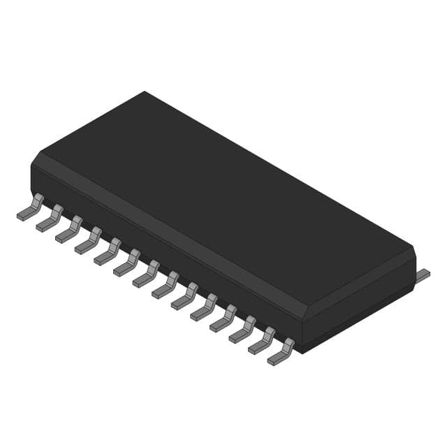
- Part No.:
- USBN9604-28MX/NOPB
- Manufacturer:
- Texas Instruments
- Category:
- Controllers
- Package:
- 28-SOIC (0.295", 7.50mm Width)
- Datasheet:
-
 USBN9604-28MX/NOPB.pdf
- Description:
- IC CONTROLLER SERIAL BUS 28-SOIC
- Quantity:
- Payment:

- Shipping:

Inventory:2,883
Please send an inquiry. Send us your inquiry, and we will respond immediately.
Product details
Overview
USBN9604-28MX/NOPB from National Semiconductor is a full-speed USB 1.1 node controller IC integrating transceiver, 3.3V regulator, Serial Interface Engine (SIE), seven endpoint FIFOs (1×8-byte control + 6×64-byte data), 8-bit parallel/MICROWIRE interface, and enhanced DMA engine. It operates at 5V or 3.3V, supports 24 MHz crystal input with internal 48 MHz PLL clock generation, and targets embedded host-peripheral bridge applications in industrial instrumentation and legacy PC peripheral controllers.
For engineers reviewing the USBN9604-28MX/NOPB datasheet, USBN9604-28MX/NOPB pinout, USBN9604-28MX/NOPB application, or USBN9604-28MX/NOPB equivalent, key selection criteria include its non-multiplexed/multiplexed CPU interface flexibility, automatic DMA (ADMA) mode for CPU-independent bulk transfers, programmable interrupt polarity, and pin-to-pin compatibility with USBN9602-28M for drop-in upgrades.
Technical Context
The USBN9604-28MX/NOPB implements a complete USB 1.1-compliant Physical Layer (PHY) and Media Access Controller (MAC) in its SIE, including NRZI decoding, bit stuffing/unstuffing, CRC generation/checking, and clock recovery from 48 MHz derived via PLL from 24 MHz input. Its transceiver meets USB 1.1 Chapter 7 electrical requirements with differential receiver, single-ended receivers (0.8–2.0 V threshold), and slew-rate-controlled transmitter.
Endpoint Pipe Controller (EPC) manages seven dedicated FIFO-based pipes: one bidirectional control endpoint (EP0) and six unidirectional endpoints (three TX, three RX), each with autonomous NAK/STALL response logic and PID toggling. The 8-bit parallel interface supports both Intel-compatible multiplexed (ALE-driven) and non-multiplexed (A0-addressed) modes selected by MODE1–MODE0 pins.
Key Specifications
| Parameter | Value and Actual Design Meaning |
|---|---|
| USB Compliance | Full-speed USB 1.0/1.1 compliant; no USB 2.0 high-speed support |
| Operating Voltage | 5.0 V or 3.3 V supply; V3.3 pin serves as regulator output or external 3.3 V input |
| Oscillator Input | 24 MHz fundamental crystal on XIN/XOUT; external 24 MHz clock also accepted |
| Internal Clock | 48 MHz generated via PLL; CLKOUT programmable (e.g., 4 MHz default post-reset) |
| FIFO Capacity | EP0: 8-byte bidirectional; EP1–EP6: 64-byte unidirectional (3 TX + 3 RX) |
| DMA Modes | Standard DMA + Automatic DMA (ADMA) enabling CPU-free 64-byte packet transfers up to 16 KB |
| Interface Modes | Non-multiplexed (MODE1–0 = 00), multiplexed (01), MICROWIRE (10); Mode 11 reserved |
Pinout & Package
USBN9604-28MX/NOPB is housed in a 28-pin SOIC (Small Outline Integrated Circuit) package with 300 mil body width, compatible with standard SO-28 PCB footprints and reflow soldering profiles.
| Pin/Terminal | Circuit Role | Design Meaning |
|---|---|---|
| VCC | Digital power supply | 5.0 V or 3.3 V main supply; power-on reset triggered at VCC ramp-up |
| GND | Digital ground reference | Common return for digital logic; separate from AGND |
| AGND | Analog ground reference | Ground return for transceiver and voltage regulator analog circuitry |
| V3.3 | Transceiver 3.3 V supply | Output of internal regulator (when enabled) or external 3.3 V input for transceiver |
| XIN / XOUT | Crystal oscillator terminals | Support 24 MHz fundamental crystal; XOUT left open for external clock input |
| CLKOUT | Programmable clock output | Configurable frequency output (e.g., 4 MHz default); stalled 214 cycles during hardware reset |
| RESET | Active-low hardware reset | Asserting RESET forces all registers to reset values and stalls CLKOUT |
| D+ / D− | USB differential data pair | Compliant full-speed transceiver I/O; D+ requires 1.5 kΩ pull-up to 3.3 V |
| CS / RD / WR | Parallel interface controls | Active-low chip select, read strobe, write strobe for non-multiplexed mode |
| A0 / D0–D7 | Address/data bus | A0 selects register address; D0–D7 carry data in non-multiplexed mode |
| MODE1 / MODE0 | Interface mode select | Hard-wired to VCC/GND to configure parallel non-mux/mux or MICROWIRE mode |
| INTR / DRQ / DACK | DMA/interrupt signals | Configurable active-high/low/open-drain INTR; DRQ/DACK enable DMA handshaking |
Key Features
| Feature | Design Value |
|---|---|
| Enhanced DMA engine | Automatic DMA (ADMA) mode transfers up to 16 KB without CPU intervention using 64-byte packets |
| Flexible CPU interface | Selectable non-multiplexed (A0-addressed) or multiplexed (ALE-latched) 8-bit parallel bus |
| Low-power operation | Fully static HALT mode with asynchronous wake-up; suitable for bus-powered devices |
| Integrated transceiver | Meets USB 1.1 Chapter 7 electrical specs; includes 3.3 V regulator and D+ pull-up support |
| Seven endpoint architecture | Dedicated FIFOs per endpoint (EP0–EP6); supports control, interrupt, bulk, and isochronous transfers |
Applications
| Industrial Data Acquisition | Legacy PC Peripheral Bridge |
|---|---|
Use Scenario: USB-connected sensor node collecting analog/digital measurements in factory-floor PLC environments. IC Role / Device Role / Timing Role: Full-speed USB node controller handling enumeration, descriptor exchange, and bulk IN transfers of sampled data. Use Value: Integrated 3.3 V regulator powers transceiver and external pull-up; ADMA offloads CPU during continuous 64-byte packet streaming. |
Use Scenario: Retrofit adapter converting RS-232 or parallel printer port to USB for legacy office equipment. IC Role / Device Role / Timing Role: USB function controller implementing CDC ACM or printer class descriptors with interrupt OUT command channel. Use Value: Pin-to-pin compatibility with USBN9602-28M enables direct replacement in existing designs; non-multiplexed interface simplifies connection to 8051-style microcontrollers. |
| Embedded Test Instrumentation | USB Firmware Programmer |
Use Scenario: Benchtop oscilloscope or logic analyzer using USB for waveform upload and remote control. IC Role / Device Role / Timing Role: Isochronous-capable node controller managing time-critical bulk IN transfers of real-time sample buffers. Use Value: Six unidirectional endpoints allow concurrent control (EP0), status polling (EP1), and high-throughput data streaming (EP2–EP4). |
Use Scenario: In-system programmer for microcontrollers with USB bootloader interface. IC Role / Device Role / Timing Role: USB device controller executing vendor-specific commands to initiate flash erase/write over bulk endpoints. Use Value: Programmable interrupt polarity (via MCNTRL register) matches host-side GPIO configuration; HALT mode reduces power during idle programming phases. |
Equivalent & Alternatives
The following parts are listed as comparable options for similar USB node controller applications.
| Alternative Part | Technical Difference | Application Difference | Selection Advice |
|---|---|---|---|
| USBN9603-28MX/NOPB | Identical functionality except clock reset mechanism; USBN9604 uses DLL-synchronized hardware reset | No functional difference in enumeration, transfer, or power modes; identical register map and timing | Select USBN9604-28MX/NOPB when DLL-based clock stability during reset is required |
| CP2102-GM | USB-to-UART bridge ASIC; no parallel/MICROWIRE host interface; integrated USB PHY only | Targets UART-based peripherals only; lacks endpoint configurability and ADMA capability | Choose CP2102-GM for simple serial bridging; USBN9604-28MX/NOPB for custom USB device firmware with CPU control |
Compared with USBN9603-28MX/NOPB, the USBN9604-28MX/NOPB offers improved clock synchronization during hardware reset, while CP2102-GM provides turnkey UART bridging but sacrifices endpoint flexibility and host-CPU interfacing capability essential for custom USB device development.
Availability
USBN9604-28MX/NOPB is available at Aetrix Electronics and suitable for industrial data acquisition, legacy peripheral bridging, and embedded test instrumentation requiring stable component supply and long-term lifecycle support.
Supply support for USBN9604-28MX/NOPB includes scheduled delivery planning, volume procurement assistance, BOM continuity management, traceable sourcing, and lifecycle availability coordination for OEM customers, industrial embedded developers, connected-device designers, and electronics production programs.
Manufacturer
National Semiconductor was a U.S.-based semiconductor company specializing in analog and interface ICs, acquired by Texas Instruments in 2011; its legacy USB controller portfolio remains widely deployed in industrial systems.
The USBN960x family was designed as a cost-optimized, full-speed USB node controller for resource-constrained embedded systems requiring minimal external components and flexible host interface options.
FAQ
What USB specification versions does the USBN9604-28MX/NOPB support?
The USBN9604-28MX/NOPB supports USB Specification versions 1.0 and 1.1 only - it is a full-speed (12 Mbps) node controller and does not implement USB 2.0 high-speed (480 Mbps) functionality. All SIE logic, transceiver behavior, and descriptor handling comply strictly with USB 1.1 requirements, including Chapter 7 electrical compliance and Chapter 8 protocol stack implementation. USBN9604-28MX/NOPB cannot enumerate or operate on USB 2.0 hubs unless operating in full-speed fallback mode.
Does the USBN9604-28MX/NOPB require an external crystal, or can it use an external clock source?
The USBN9604-28MX/NOPB accepts either a 24 MHz fundamental crystal connected between XIN and XOUT, or a 24 MHz square-wave clock signal applied to XIN with XOUT left unconnected. The internal oscillator circuit is optimized for AT-cut crystals with 20 pF load capacitance and ≤50 Ω series resistance. Using an external clock eliminates crystal layout sensitivity but requires tight signal integrity control on the XIN trace to avoid jitter-induced USB packet errors. USBN9604-28MX/NOPB does not support frequencies other than 24 MHz for clock input.
How does the Automatic DMA (ADMA) mode function in the USBN9604-28MX/NOPB?
ADMA mode in the USBN9604-28MX/NOPB enables fully CPU-independent USB data transfers by chaining 64-byte packets up to 16 KB total (256 × 64 bytes). Once configured via DMACNTRL and DMACNT registers, the ADMA engine handles PID toggling, NAK recovery, and FIFO servicing without software intervention. This allows the host microcontroller to enter low-power states or service other tasks during sustained bulk transfers - a critical advantage in battery-powered or real-time embedded USBN9604-28MX/NOPB implementations.
What is the purpose of the V3.3 pin on the USBN9604-28MX/NOPB, and how should it be decoupled?
The V3.3 pin on the USBN9604-28MX/NOPB serves as either the output of the internal 3.3 V regulator (when enabled) or as an external 3.3 V supply input for the transceiver. When used as regulator output, it must be decoupled with a 1 µF tantalum capacitor to AGND - ceramic capacitors are insufficient due to ESR requirements specified in the datasheet. If the system operates at 3.3 V and the regulator is disabled, V3.3 becomes an input requiring clean, low-noise 3.3 V supply. USBN9604-28MX/NOPB's transceiver will not function without proper biasing of this pin.
Is the USBN9604-28MX/NOPB pin-compatible with the earlier USBN9602-28M device?
Yes - the USBN9604-28MX/NOPB is explicitly documented as pin-to-pin compatible with USBN9602-28M in the "Available in two packages" section of the datasheet, supporting drop-in replacement in existing SO-28 layouts. All signal names, pin positions, and DC/AC timing parameters match. However, USBN9604-28MX/NOPB adds DLL-based clock synchronization during hardware reset, which improves timing stability but does not affect pin-level interoperability. No PCB changes are required when upgrading from USBN9602-28M to USBN9604-28MX/NOPB.
USBN9604-28MX/NOPB Specifications
- Product attributes
- Attribute value
- Manufacturer:
- Texas Instruments
- Package/Case:
- 28-SOIC (0.295", 7.50mm Width)
- Programmable:
- Not Verified
- Protocol:
- USB
- Function:
- Controller
- Interface:
- Parallel
- Standards:
- USB 1.0 and 1.1
- Voltage - Supply:
- 3V ~ 5.5V
- Current - Supply:
- 30mA
- Operating Temperature:
- 0°C ~ 70°C
- Supplier Device Package:
- 28-SOIC
- Grade:
- -
- Qualification:
- -
USBN9604-28MX/NOPB FAQ
1.How can I place an order for USBN9604-28MX/NOPB through Aetrix?
Please submit a Request for Quotation (RFQ) for USBN9604-28MX/NOPB on Aetrix. Our sales agent will provide a competitive quotation and guide you through the order confirmation once you accept the terms.
2.Are the price and stock information for USBN9604-28MX/NOPB reliable?
The price and inventory of USBN9604-28MX/NOPB are updated periodically and may fluctuate due to market conditions. Stock and pricing data are typically refreshed every 24 hours. Quotation validity for USBN9604-28MX/NOPB is usually 5 days.
3.What payment methods are accepted for USBN9604-28MX/NOPB?
We accept Wire Transfer, PayPal, Credit Card, Western Union, MoneyGram, and Escrow for USBN9604-28MX/NOPB transactions.
Note: Certain payment methods may incur a processing fee.
4.How is shipping managed for USBN9604-28MX/NOPB?
USBN9604-28MX/NOPB orders can be shipped via leading logistics carriers, including DHL, UPS, FedEx, TNT, or Registered Mail.
Once your USBN9604-28MX/NOPB order is processed, you will receive an email with the shipment details and tracking number.
Note: Tracking information may take up to 24 hours to appear. Express delivery typically takes 3–5 business days.
5.How can I obtain technical support or documentation for USBN9604-28MX/NOPB?
For technical support, including USBN9604-28MX/NOPB datasheets, pinout diagrams, or application guidance, please contact our engineering support team. They can provide detailed documentation and assistance for your USBN9604-28MX/NOPB requirements.
6.How does Aetrix verify that USBN9604-28MX/NOPB is sourced from the original manufacturer or authorized distributors?
All USBN9604-28MX/NOPB products on Aetrix are procured from qualified distributors and authorized channels. Our dedicated quality assurance team conducts strict verification, including traceability checks and, if necessary, third-party testing. This ensures that USBN9604-28MX/NOPB meets industry standards.
7.What is the process for return or replacement of USBN9604-28MX/NOPB?
All USBN9604-28MX/NOPB units undergo pre-shipment inspection (PSI). If there is an issue with USBN9604-28MX/NOPB, returns or replacements are accepted under the following conditions:
1.Quantity discrepancies, incorrect items, or visible external defects (such as breakage or corrosion), acknowledged by Aetrix.
2.The issue is reported within 90 days of delivery.
3.The USBN9604-28MX/NOPB part is unused and in its original packaging.
Return procedure for USBN9604-28MX/NOPB:
1.Submit a request within 90 days.
2.Obtain a Return Material Authorization (RMA) from Aetrix.
USBN9604-28MX/NOPB Tags

-
PTN5150AHXMP
NXP Semiconductors

-
USB3740B-AI9-TR
Microchip Technology

-
USB3740B-AI2-TR
Microchip Technology

-
USB3300-EZK-TR
Microchip Technology
-
USB3300-EZK
Microchip Technology

-
FUSB340TMX
onsemi

-
FUSB302BMPX
onsemi

-
DP83826IRHBR
Texas Instruments

-
MCP2518FDT-E/QBB
Microchip Technology
-
FUSB302MPX
onsemi

-
MCP2518FDT-E/SL
Microchip Technology

-
FT260Q-R
FTDI, Future Technology Devices International Ltd
Tech Hub

A practical engineering guide to 3.3V and 5V logic compatibility, input thresholds, resistor dividers, translator ICs, MOSFET level shifting, I2C pull-ups, timing limits and power-sequencing risks.

The 74HC595 uses push-pull logic outputs, while the TPIC6B595 uses 50 V open-drain DMOS sinks for higher-power loads. This guide compares timing, current limits, 3.3 V interfacing, load wiring, thermal…

The 74HC595 converts serial data into eight stable parallel outputs. This guide covers pin functions, shift and storage timing, OE and MR behavior, drive-current limits, cascading, voltage compatibilit…

A technical comparison of level-sensitive latches and edge-triggered flip-flops, covering timing windows, setup and hold limits, master–slave operation, time borrowing, race-through, HDL inference and…

A D latch stores one bit while Enable controls when data can pass. This reference covers gate-level operation, truth tables, transparency, setup and hold timing, LE versus OE, common ICs and practical …

An SR latch stores one bit through cross-coupled feedback. This engineering reference covers NOR and NAND implementations, truth tables, forbidden-state recovery, gated operation, switch debouncing, fa…

Latch circuits retain one bit through feedback. This technical reference covers SR and D latches, truth tables, transparency, timing limits, latch-versus-flip-flop behavior, applications and common log…

An engineering guide to LED driver operation, constant-current and constant-voltage outputs, linear and switching topologies, dimming, IC selection, calculations, replacement compatibility, and fault c…

Operational amplifier guide covering op amp basics, feedback, ideal vs real op amps, common configurations, buffer circuits, offset, bias current, gain-bandwidth, slew rate, rail-to-rail limits and sel…

Jumper cables guide covering safe connection order, red and black clamp placement, final ground connection, cable gauge, length, clamp quality, copper vs CCA cables, jump starter comparison and battery…


