
 My Inquiry
 My Account


Texas Instruments USBN9604SLB/NOPB
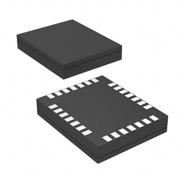
- Part No.:
- USBN9604SLB/NOPB
- Manufacturer:
- Texas Instruments
- Category:
- Controllers
- Package:
- 28-TFQFN, CSP
- Datasheet:
-
 USBN9604SLB/NOPB.pdf
- Description:
- IC CTRLR FULL SPEED 28-LAMCSP
- Quantity:
- Payment:

- Shipping:

Inventory:250
Please send an inquiry. Send us your inquiry, and we will respond immediately.
Product details
Overview
USBN9604SLB/NOPB from National Semiconductor is a full-speed USB 1.1 node controller IC integrating transceiver, 3.3V regulator, Serial Interface Engine (SIE), seven endpoint FIFOs (1×8-byte control + 6×64-byte data), 8-bit parallel/MICROWIRE interface, and enhanced DMA engine. It operates at 5V or 3.3V, supports 24 MHz crystal input with internal 48 MHz PLL clock generation, and targets embedded peripheral connectivity in industrial controllers and portable USB devices.
For engineers reviewing the USBN9604SLB/NOPB datasheet, USBN9604SLB/NOPB pinout, USBN9604SLB/NOPB application, or USBN9604SLB/NOPB equivalent, key selection criteria include endpoint FIFO depth, ADMA mode support for CPU-independent bulk transfers, programmable interrupt polarity, non-multiplexed/multiplexed bus interface flexibility, and integrated 3.3V transceiver regulation.
Technical Context
The USBN9604SLB/NOPB implements a complete USB 1.1-compliant physical layer (PHY) and media access controller (MAC) within its SIE, including NRZI decoding, bit stuffing/unstuffing, CRC generation/checking, and clock recovery from 48 MHz derived from a 24 MHz oscillator. Its endpoint pipe controller (EPC) manages seven bidirectional/unidirectional pipes with dedicated FIFOs and automatic NAK/STALL response logic.
It features two distinct DMA modes: standard DMA with external controller coordination and Automatic DMA (ADMA), enabling fully CPU-independent transfer of up to 16 KB (256 × 64-byte packets) with automatic PID toggling and NAK recovery. The MICROWIRE/PLUS interface provides serial CPU connectivity when parallel bus resources are constrained.
Key Specifications
| Parameter | Value and Actual Design Meaning |
|---|---|
| USB Compliance | Full-speed USB 1.0/1.1 compliant; no high-speed (USB 2.0) support. |
| Endpoint Pipes | 7 total: EP0 (bidirectional, 8-byte FIFO) + 3 TX + 3 RX (each 64-byte FIFO). |
| Interface Modes | Non-multiplexed parallel, multiplexed (Intel-compatible), or MICROWIRE/PLUS serial. |
| DMA Capability | Automatic DMA (ADMA) mode transfers up to 16 KB without CPU intervention. |
| Power Supply | Single 5V or 3.3V operation; internal 3.3V regulator for transceiver (V3.3 pin). |
| Clock Source | 24 MHz crystal or external clock on XIN; internal PLL generates 48 MHz for SIE. |
| Operating Temp | –40°C to +85°C industrial temperature range per datasheet specifications. |
Pinout & Package
USBN9604SLB/NOPB uses a 28-pin CSP (Chip Scale Package) with 0.5 mm pitch, optimized for compact portable designs. Pin functions are validated per National Semiconductor SNOS528L Rev 1.3 (June 2003), Section 1.2.
| Pin/Terminal | Circuit Role | Design Meaning |
|---|---|---|
| RESET | Hardware reset input | Active-low signal that resets all registers, stalls CLKOUT for 214 XIN cycles, and disables V3.3 regulator. |
| XIN / XOUT | Oscillator interface | Supports 24 MHz fundamental crystal; XOUT left unconnected if external 24 MHz clock is used. |
| CLKOUT | Programmable clock output | Configurable via CCONF register; defaults to 4 MHz after reset; stalls during DLL sync in USBN9604. |
| D+ / D− | USB differential pair | Integrated transceiver I/O; requires 1.5 kΩ pull-up on D+ to V3.3 for full-speed enumeration. |
| V3.3 | Transceiver voltage supply | Output of internal 3.3V regulator (when enabled) or 3.3V input (when disabled); requires 1 µF decoupling. |
| MODE1–0 | Interface mode select | Hard-wired pins: 00=non-mux, 01=mux, 10=MICROWIRE, 11=reserved. |
| INTR | Configurable interrupt | Software-programmable active-high/low/push-pull/open-drain; tri-stated during reset. |
| DRQ / DACK | DMA handshake | DRQ asserts request; DACK acknowledges transfer completion - both active-low and DMA-only. |
Key Features
| Feature | Design Value |
|---|---|
| Enhanced DMA engine | ADMA mode enables autonomous 64-byte packet transfers up to 16 KB, eliminating CPU polling overhead for bulk/isochronous traffic. |
| Dedicated endpoint FIFOs | Separate 64-byte TX/RX FIFOs per non-control endpoint ensure deterministic latency and prevent inter-endpoint data corruption. |
| Flexible microcontroller interface | Three hardware-selectable modes (non-mux/mux/MICROWIRE) allow direct integration with diverse MCU families without glue logic. |
| Integrated 3.3V regulator | On-chip regulator powers transceiver and external D+ pull-up, reducing BOM count and simplifying 5V-system design. |
| Low-power HALT mode | Fully static HALT with asynchronous wake-up supports bus-powered operation while minimizing standby current. |
Applications
| Industrial Human-Machine Interface (HMI) | Medical Data Logger |
|---|---|
Use Scenario: USB-connected touch panel or keypad in factory-floor control cabinet requiring reliable plug-and-play enumeration under EMI stress. IC Role / Device Role / Timing Role: Full-speed USB node controller handling HID-class control transfers and interrupt IN reports from buttons/sensors. Use Value: Integrated transceiver and 3.3V regulator eliminate external level-shifting components; ADMA offloads firmware during burst log uploads. | Use Scenario: Portable patient monitor collecting ECG/SpO₂ data and uploading to host PC via USB cable. IC Role / Device Role / Timing Role: USB function controller managing isochronous audio streaming and bulk data transfers to host storage. Use Value: Six dedicated 64-byte FIFOs enable concurrent real-time sensor streaming and buffered file writes without CPU contention. |
| Embedded Test Equipment | USB-to-Parallel Bridge Module |
Use Scenario: Benchtop oscilloscope or power analyzer using USB for remote command/control and waveform data export. IC Role / Device Role / Timing Role: USB device controller implementing vendor-specific class for instrument command parsing and bulk waveform readback. Use Value: Non-multiplexed 8-bit interface simplifies connection to FPGA-based control logic; programmable INTR polarity matches legacy host driver requirements. | Use Scenario: Legacy parallel-port peripheral (e.g., printer, scanner) retrofitted with USB connectivity via bridge board. IC Role / Device Role / Timing Role: USB node controller acting as bridge endpoint, translating USB OUT tokens into parallel strobes and ACKs. Use Value: MICROWIRE interface allows direct connection to low-pin-count microcontrollers; HALT mode reduces power during idle periods between print jobs. |
Equivalent & Alternatives
The following parts are listed as comparable options for similar USB node controller applications.
| Alternative Part | Technical Difference | Application Difference | Selection Advice |
|---|---|---|---|
| USBN9603SLB/NOPB | Identical functionality and pinout; differs only in reset mechanism for clock generation circuit (USBN9604 includes hardware reset synchronization with DLL lock). | Same USB 1.1 node role; suitable where precise clock stability post-reset is critical (e.g., synchronized multi-device systems). | Select USBN9604SLB/NOPB when DLL lock timing predictability is required; USBN9603SLB/NOPB suffices for general-purpose enumeration. |
| ISP1181BD | Philips USB 1.1 device controller; supports same 7 endpoints but lacks integrated 3.3V regulator and ADMA mode - requires external regulator and external DMA controller. | Requires additional power management IC and DMA logic; higher BOM cost and PCB area vs. USBN9604SLB/NOPB's single-chip solution. | Choose USBN9604SLB/NOPB for lowest component count and autonomous DMA; ISP1181BD only if existing design already uses Philips ecosystem. |
Compared with USBN9603SLB/NOPB, the USBN9604SLB/NOPB adds DLL-synchronized hardware reset behavior for improved clock stability, while versus ISP1181BD it delivers integrated regulation and true CPU-independent ADMA - reducing system-level complexity and component count in space-constrained embedded USB peripherals.
Availability
USBN9604SLB/NOPB is available at Aetrix Electronics and suitable for industrial HMI, medical data loggers, and embedded test equipment requiring stable component supply, long-lifecycle support, and verified USB 1.1 compliance.
Supply support for USBN9604SLB/NOPB includes scheduled delivery planning, volume procurement assistance, BOM continuity management, traceable sourcing, and lifecycle availability coordination for OEM customers, industrial embedded developers, connected-device designers, and electronics production programs.
Manufacturer
National Semiconductor was a U.S.-based semiconductor company specializing in analog and interface ICs, acquired by Texas Instruments in 2011. Its legacy USB controllers remain widely deployed in industrial and medical systems.
The USBN960x family was designed as a cost-optimized, single-chip USB 1.1 node solution for resource-constrained microcontroller-based peripherals - emphasizing integration (transceiver + regulator + SIE + DMA), low EMI, and flexible host interface options.
FAQ
What USB specification versions does the USBN9604SLB/NOPB support?
The USBN9604SLB/NOPB supports USB Specification versions 1.0 and 1.1 only - it is a full-speed (12 Mbps), not high-speed (480 Mbps), USB device controller. It does not implement USB 2.0 or later protocols. All functional blocks - including the Serial Interface Engine, transceiver, and endpoint logic - are validated against USB 1.1 compliance requirements per the official National Semiconductor datasheet SNOS528L.
Does the USBN9604SLB/NOPB require an external crystal, or can it use an external clock source?
The USBN9604SLB/NOPB supports both configurations: a 24 MHz fundamental crystal connected between XIN and XOUT, or a 24 MHz CMOS-level clock signal applied solely to XIN (with XOUT left unconnected). The internal oscillator circuit and PLL are designed exclusively for 24 MHz input; deviation invalidates USB timing compliance. The USBN9604SLB/NOPB datasheet specifies ±2500 ppm crystal tolerance and recommends 1 MΩ R1 and 15 pF C1/C2 for typical crystal layouts.
How does the Automatic DMA (ADMA) mode in the USBN9604SLB/NOPB differ from standard DMA?
Standard DMA in the USBN9604SLB/NOPB requires external controller coordination for each 64-byte packet transfer, while ADMA mode enables fully autonomous movement of up to 16 KB (256 × 64-byte packets) without CPU intervention. ADMA handles PID toggling, NAK recovery, and endpoint handshaking internally - freeing the host MCU to perform other tasks during large bulk or isochronous transfers. This behavior is confirmed in Section 4.2 of the USBN9604SLB/NOPB datasheet SNOS528L.
Can the USBN9604SLB/NOPB operate from a 3.3V supply only, without using its internal regulator?
Yes - the USBN9604SLB/NOPB supports pure 3.3V operation. In this mode, the internal 3.3V regulator is disabled, and the V3.3 pin must be driven externally with a stable 3.3V supply to power the integrated transceiver. The device's core logic (VCC) still requires 3.3V, and all I/O tolerances (including D+, D−, and parallel interface) are specified for 3.3V operation. This configuration eliminates regulator overhead and is explicitly supported per Section 2.2 of the USBN9604SLB/NOPB datasheet.
What is the purpose of the MODE1–0 pins on the USBN9604SLB/NOPB, and what happens if they are left floating?
The MODE1–0 pins configure the USBN9604SLB/NOPB's host interface: 00=non-multiplexed, 01=multiplexed, 10=MICROWIRE, 11=reserved. They must be hard-wired to VCC or GND - floating states cause undefined interface behavior and failed initialization. National Semiconductor specifies this in Section 1.2.4 of the USBN9604SLB/NOPB datasheet, noting that improper biasing prevents register access and USB enumeration. No internal pull-ups or pull-downs exist on these pins.
USBN9604SLB/NOPB Specifications
- Product attributes
- Attribute value
- Manufacturer:
- Texas Instruments
- Package/Case:
- 28-TFQFN, CSP
- Programmable:
- Not Verified
- Protocol:
- USB
- Function:
- Controller
- Interface:
- Parallel
- Standards:
- USB 1.0 and 1.1
- Voltage - Supply:
- 3V ~ 5.5V
- Current - Supply:
- 30mA
- Operating Temperature:
- 0°C ~ 70°C
- Supplier Device Package:
- 28-CSP (5.5x4.5)
- Grade:
- -
- Qualification:
- -
USBN9604SLB/NOPB FAQ
1.How can I place an order for USBN9604SLB/NOPB through Aetrix?
Please submit a Request for Quotation (RFQ) for USBN9604SLB/NOPB on Aetrix. Our sales agent will provide a competitive quotation and guide you through the order confirmation once you accept the terms.
2.Are the price and stock information for USBN9604SLB/NOPB reliable?
The price and inventory of USBN9604SLB/NOPB are updated periodically and may fluctuate due to market conditions. Stock and pricing data are typically refreshed every 24 hours. Quotation validity for USBN9604SLB/NOPB is usually 5 days.
3.What payment methods are accepted for USBN9604SLB/NOPB?
We accept Wire Transfer, PayPal, Credit Card, Western Union, MoneyGram, and Escrow for USBN9604SLB/NOPB transactions.
Note: Certain payment methods may incur a processing fee.
4.How is shipping managed for USBN9604SLB/NOPB?
USBN9604SLB/NOPB orders can be shipped via leading logistics carriers, including DHL, UPS, FedEx, TNT, or Registered Mail.
Once your USBN9604SLB/NOPB order is processed, you will receive an email with the shipment details and tracking number.
Note: Tracking information may take up to 24 hours to appear. Express delivery typically takes 3–5 business days.
5.How can I obtain technical support or documentation for USBN9604SLB/NOPB?
For technical support, including USBN9604SLB/NOPB datasheets, pinout diagrams, or application guidance, please contact our engineering support team. They can provide detailed documentation and assistance for your USBN9604SLB/NOPB requirements.
6.How does Aetrix verify that USBN9604SLB/NOPB is sourced from the original manufacturer or authorized distributors?
All USBN9604SLB/NOPB products on Aetrix are procured from qualified distributors and authorized channels. Our dedicated quality assurance team conducts strict verification, including traceability checks and, if necessary, third-party testing. This ensures that USBN9604SLB/NOPB meets industry standards.
7.What is the process for return or replacement of USBN9604SLB/NOPB?
All USBN9604SLB/NOPB units undergo pre-shipment inspection (PSI). If there is an issue with USBN9604SLB/NOPB, returns or replacements are accepted under the following conditions:
1.Quantity discrepancies, incorrect items, or visible external defects (such as breakage or corrosion), acknowledged by Aetrix.
2.The issue is reported within 90 days of delivery.
3.The USBN9604SLB/NOPB part is unused and in its original packaging.
Return procedure for USBN9604SLB/NOPB:
1.Submit a request within 90 days.
2.Obtain a Return Material Authorization (RMA) from Aetrix.
USBN9604SLB/NOPB Tags

-
PTN5150AHXMP
NXP Semiconductors

-
USB3740B-AI9-TR
Microchip Technology

-
USB3740B-AI2-TR
Microchip Technology

-
USB3300-EZK-TR
Microchip Technology
-
USB3300-EZK
Microchip Technology

-
FUSB340TMX
onsemi

-
FUSB302BMPX
onsemi

-
DP83826IRHBR
Texas Instruments

-
MCP2518FDT-E/QBB
Microchip Technology
-
FUSB302MPX
onsemi

-
MCP2518FDT-E/SL
Microchip Technology

-
FT260Q-R
FTDI, Future Technology Devices International Ltd
Tech Hub

A practical engineering guide to 3.3V and 5V logic compatibility, input thresholds, resistor dividers, translator ICs, MOSFET level shifting, I2C pull-ups, timing limits and power-sequencing risks.

The 74HC595 uses push-pull logic outputs, while the TPIC6B595 uses 50 V open-drain DMOS sinks for higher-power loads. This guide compares timing, current limits, 3.3 V interfacing, load wiring, thermal…

The 74HC595 converts serial data into eight stable parallel outputs. This guide covers pin functions, shift and storage timing, OE and MR behavior, drive-current limits, cascading, voltage compatibilit…

A technical comparison of level-sensitive latches and edge-triggered flip-flops, covering timing windows, setup and hold limits, master–slave operation, time borrowing, race-through, HDL inference and…

A D latch stores one bit while Enable controls when data can pass. This reference covers gate-level operation, truth tables, transparency, setup and hold timing, LE versus OE, common ICs and practical …

An SR latch stores one bit through cross-coupled feedback. This engineering reference covers NOR and NAND implementations, truth tables, forbidden-state recovery, gated operation, switch debouncing, fa…

Latch circuits retain one bit through feedback. This technical reference covers SR and D latches, truth tables, transparency, timing limits, latch-versus-flip-flop behavior, applications and common log…

An engineering guide to LED driver operation, constant-current and constant-voltage outputs, linear and switching topologies, dimming, IC selection, calculations, replacement compatibility, and fault c…

Operational amplifier guide covering op amp basics, feedback, ideal vs real op amps, common configurations, buffer circuits, offset, bias current, gain-bandwidth, slew rate, rail-to-rail limits and sel…

Jumper cables guide covering safe connection order, red and black clamp placement, final ground connection, cable gauge, length, clamp quality, copper vs CCA cables, jump starter comparison and battery…


