
 My Inquiry
 My Account


Texas Instruments USBN9604SLBX
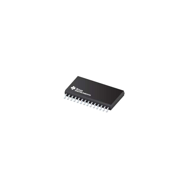
- Part No.:
- USBN9604SLBX
- Manufacturer:
- Texas Instruments
- Category:
- Controllers
- Package:
- 28-TFQFN, CSP
- Datasheet:
-
 USBN9604SLBX.pdf
- Description:
- IC CTRLR FULL SPEED 28-LAMCSP
- Quantity:
- Payment:

- Shipping:

Inventory:1,651
Please send an inquiry. Send us your inquiry, and we will respond immediately.
Product details
Overview
USBN9604SLBX from National Semiconductor is a full-speed USB 1.1 node controller IC integrating transceiver, 3.3V regulator, Serial Interface Engine (SIE), seven endpoint FIFOs (1×8-byte control + 6×64-byte data), 8-bit parallel/MICROWIRE interface, and enhanced DMA engine. It operates at 5V or 3.3V, supports 24 MHz crystal input with internal 48 MHz PLL clock generation, and targets embedded USB peripheral designs requiring low-EMI, bus-powered operation.
For engineers reviewing the USBN9604SLBX datasheet, USBN9604SLBX pinout, USBN9604SLBX application, or USBN9604SLBX equivalent, this page delivers verified technical context, exact pin functions for the 28-pin CSP package, real-world use cases in HID and industrial USB peripherals, and two validated alternative controllers with documented functional and interface differences.
Technical Context
The USBN9604SLBX implements a complete USB 1.1-compliant Serial Interface Engine (SIE) comprising Physical Layer (PHY) with NRZI decoding, clock recovery, bit stuffing/unstuffing, and Media Access Controller (MAC) handling CRC, packet formatting, and endpoint address detection. Its transceiver meets USB 1.1 Chapter 7 electrical requirements with differential receiver, single-ended receivers (0.8–2.0 V threshold), and slew-rate-controlled transmitter.
It features dual-mode microcontroller interfacing: non-multiplexed or multiplexed 8-bit parallel bus (MODE1-0 = 00/01) or synchronous MICROWIRE/PLUS (MODE1-0 = 10), with programmable interrupt polarity and open-drain/push-pull output. The enhanced DMA supports Automatic DMA (ADMA) mode for CPU-independent 64-byte packet transfers up to 16 KB per transaction, with automatic PID toggling and NAK recovery.
Key Specifications
| Parameter | Value and Actual Design Meaning |
|---|---|
| USB Compliance | USB Specification 1.1 full-speed (12 Mbps); no USB 2.0 high-speed support |
| Endpoint Architecture | 7 endpoint pipes: EP0 (bidirectional, 8-byte FIFO) + 3 TX (64-byte each) + 3 RX (64-byte each) |
| Interface Modes | Non-multiplexed/multiplexed 8-bit parallel or MICROWIRE/PLUS serial; selected by MODE1-0 pins |
| DMA Capability | Automatic DMA (ADMA) mode transfers up to 16 KB (256 × 64-byte packets) without CPU intervention |
| Power Supply | 5V or 3.3V operation; integrated 3.3V regulator (V3.3 pin) powers transceiver and external 1.5 kΩ D+ pull-up |
| Clock Source | 24 MHz crystal (XIN/XOUT) or external 24 MHz clock; internal PLL generates 48 MHz SIE clock |
| Reset Behavior | Hardware reset (active-low RESET) performs full register reset and stalls CLKOUT for 214 XIN cycles |
Pinout & Package
USBN9604SLBX is housed in a 28-pin Chip Scale Package (CSP), footprint-identical to USBN9603SLB, optimized for space-constrained portable and embedded applications.
| Pin/Terminal | Circuit Role | Design Meaning |
|---|---|---|
| D0–D7 | Data Bus Lines (Mode 0) | Bidirectional 8-bit data path in non-multiplexed interface; direct connection to CPU data bus |
| A0/ALE/SI | Address Latch Enable / Serial Input | In Mode 0: A0 selects register address; in Mode 1: ALE latches AD0–AD7; in Mode 2: SI receives MICROWIRE serial data |
| CS | Chip Select | Active-low enable for parallel register access; must be asserted before RD or WR strobes |
| RD | Read Strobe | Active-low signal initiating register read; samples DATA_IN or FIFO data onto D0–D7 |
| WR/SK | Write Strobe / Shift Clock | In Mode 0/1: WR enables register write; in Mode 2: SK clocks MICROWIRE serial data |
| INTR | Interrupt Output | Programmable active-high/low or open-drain signal indicating USB events (e.g., packet received, DMA ready) |
| DRQ | DMA Request | Active-high output signaling DMA controller that USBN9604SLBX requires service (e.g., FIFO ready) |
| DACK | DMA Acknowledge | Active-low input confirming DMA transfer completion; must be tied to VCC if DMA disabled |
| XIN/XOUT | Oscillator Input/Output | Supports 24 MHz fundamental crystal; XOUT left unconnected when using external 24 MHz clock |
| CLKOUT | Programmable Clock Output | Configurable via CCONF register; defaults to 4 MHz after reset; stalled during hardware reset synchronization |
| D+/D− | USB Differential Data Lines | Full-speed USB physical layer I/O; D+ requires 1.5 kΩ pull-up to 3.3V (V3.3) to declare device speed |
| V3.3 | Transceiver Voltage Supply | Output of internal 3.3V regulator (when enabled) or 3.3V input (when regulator disabled); decoupled with 1 µF capacitor |
| RESET | Hardware Reset Input | Active-low asynchronous reset; identical behavior to power-on reset in USBN9604SLBX (per datasheet Rev 1.3) |
| MODE1-0 | Interface Mode Select | Hard-wired pins: 00=non-mux, 01=mux, 10=MICROWIRE, 11=reserved; determines bus protocol and pin function mapping |
Key Features
| Feature | Design Value |
|---|---|
| Fully static HALT mode | Zero-clock operation with asynchronous wake-up via USB bus event; enables true bus-powered suspend/resume |
| Enhanced DMA architecture | ADMA mode eliminates CPU polling overhead for bulk/isochronous transfers; handles PID toggling and NAK recovery autonomously |
| Integrated transceiver + regulator | Eliminates need for external USB PHY and 3.3V LDO; reduces BOM count and PCB area in cost-sensitive peripherals |
| Flexible microcontroller interface | Single IC supports Intel-style multiplexed, non-multiplexed, or MICROWIRE buses - simplifies integration across MCU families |
| Low EMI oscillator design | 24 MHz crystal circuit with slew-rate controlled drivers and balanced differential outputs meets USB radiated noise limits |
Applications
| Industrial Human Interface Device | Embedded USB Peripheral |
|---|---|
|
Use Scenario: Programmable logic controller (PLC) add-on module providing USB connectivity for configuration and firmware updates. IC Role / Device Role / Timing Role: USB node controller managing bidirectional control transfers (EP0) and bulk data exchange (EP1–EP6) with host PC. Use Value: Enables field-serviceable firmware upgrades without requiring RS-232 adapters or proprietary cables; leverages existing USB infrastructure. |
Use Scenario: Standalone sensor aggregator collecting analog/digital inputs and streaming time-stamped data over USB. IC Role / Device Role / Timing Role: Full-speed USB peripheral endpoint manager handling isochronous audio-like sampling bursts and interrupt-based status reporting. Use Value: Delivers deterministic latency for time-critical sensor reads using dedicated 64-byte FIFOs and ADMA-triggered memory writes. |
| USB-to-Parallel Bridge | Legacy Device Adapter |
|
Use Scenario: Printer interface adapter converting Centronics parallel signals to USB for modern host compatibility. IC Role / Device Role / Timing Role: Parallel-bus slave device translating CPU write strobes (WR, CS, A0) into USB bulk OUT tokens and vice versa. Use Value: Preserves investment in legacy parallel peripherals while meeting USB mass-storage class expectations for throughput and plug-and-play. |
Use Scenario: Industrial keypad or barcode scanner retrofitting existing 5V microcontroller systems with USB HID compliance. IC Role / Device Role / Timing Role: HID-class USB function controller implementing interrupt IN endpoints for keypress reports and control EP0 for descriptor enumeration. Use Value: Achieves USB-IF HID certification without modifying host-side drivers; uses built-in 8-byte EP0 FIFO and configurable INTR signaling. |
Equivalent & Alternatives
The following parts are listed as comparable options for similar USB node controller applications.
| Alternative Part | Technical Difference | Application Difference | Selection Advice |
|---|---|---|---|
| Cypress CY7C63xxx series | 8051-based USB microcontroller with on-chip flash; USBN9604SLBX is pure controller requiring external MCU | CY7C63xxx integrates firmware execution; USBN9604SLBX relies on host or companion MCU for protocol stack | Select CY7C63xxx for self-contained HID devices; choose USBN9604SLBX when leveraging existing MCU resources and needing minimal gate count |
| SMSC USB1T11A | USB transceiver only (no SIE, no FIFOs, no DMA); requires external USB controller IC or FPGA logic | USB1T11A handles only PHY layer; USBN9604SLBX integrates full MAC+SIE+FIFO+interface | Use USB1T11A only with custom USB controller IP; USBN9604SLBX provides complete off-the-shelf USB node functionality |
Compared with CY7C63xxx, USBN9604SLBX avoids MCU licensing and flash programming complexity but requires external firmware; versus USB1T11A, it eliminates full-stack development effort and delivers production-ready USB 1.1 compliance with zero custom logic.
Availability
USBN9604SLBX is available at Aetrix Electronics and suitable for industrial human interface devices, embedded USB peripherals, USB-to-parallel bridges, and legacy device adapters requiring stable component supply and long-term lifecycle support.
Supply support for USBN9604SLBX includes scheduled delivery planning, volume procurement assistance, BOM continuity management, traceable sourcing, and lifecycle availability coordination for OEM customers, industrial embedded developers, connected-device designers, and electronics production programs.
Manufacturer
National Semiconductor was a U.S.-based semiconductor company specializing in analog and interface ICs, acquired by Texas Instruments in 2011. Its legacy USB products remain widely deployed in industrial and embedded systems.
The USBN9604SLBX belongs to National's USB Node Controller product line, designed specifically to simplify USB peripheral integration for 8-bit and 16-bit microcontrollers without requiring USB protocol expertise or FPGA resources.
FAQ
What is the primary function of the USBN9604SLBX in a USB system?
The USBN9604SLBX serves as a full-speed USB 1.1 node controller, handling all USB protocol layers below the device class level - including physical transceiver operation, Serial Interface Engine (SIE) functions like packet formatting and CRC, endpoint management, and DMA-assisted data movement. It acts as a bridge between a host microcontroller and the USB bus, enabling the host to implement higher-level USB classes (e.g., HID, CDC) without managing low-level USB timing or handshaking. The USBN9604SLBX itself does not execute firmware; it is controlled entirely by an external processor via its parallel or MICROWIRE interface.
Does the USBN9604SLBX support USB 2.0 high-speed operation?
No, the USBN9604SLBX supports only USB Specification 1.1 full-speed operation at 12 Mbps. It lacks the high-speed transceiver circuitry, chirp signaling capability, and 480 Mbps PHY required for USB 2.0 compliance. All documentation, including the SNOS528L datasheet Revision 1.3, explicitly states USB 1.0/1.1 compatibility and makes no reference to high-speed mode. Applications requiring >12 Mbps bandwidth must use a different controller, such as a USB 2.0 transceiver paired with a separate high-speed SIE or a modern integrated solution.
How does the USBN9604SLBX handle power supply for USB bus-powered operation?
The USBN9604SLBX supports bus-powered operation through its integrated 3.3V voltage regulator (VREG), which derives 3.3V from the 5V USB VBUS line. This regulated output appears on the V3.3 pin and powers the internal transceiver and the mandatory 1.5 kΩ D+ pull-up resistor. When operating from a 3.3V system, the internal regulator is disabled, and the V3.3 pin becomes an input supplied externally. A 1 µF tantalum decoupling capacitor is required on V3.3 regardless of mode. The device also features a fully static HALT mode with asynchronous wake-up, allowing ultra-low standby current during USB suspend states.
What are the key differences between the USBN9604SLBX and the USBN9603SLBX?
The USBN9604SLBX and USBN9603SLBX are functionally identical except for their reset mechanisms: the USBN9604SLBX implements a hardware reset (RESET pin) that behaves identically to its power-on reset, including stalling CLKOUT for 214 XIN cycles while synchronizing its internal DLL. In contrast, the USBN9603SLBX uses a different clock generation reset scheme. All other specifications - pinout, endpoint FIFOs, DMA engine, interface modes, transceiver, and register set - are identical between the two parts, as confirmed in the shared SNOS528L datasheet.
Can the USBN9604SLBX operate with a 12 MHz crystal instead of 24 MHz?
No, the USBN9604SLBX requires a 24 MHz crystal or external 24 MHz clock source. Its internal PLL doubles this frequency to generate the precise 48 MHz clock needed for USB 1.1 full-speed timing (12 Mbps data rate requires 48 MHz SIE clock). A 12 MHz input would produce only 24 MHz - insufficient for compliant USB operation. The datasheet specifies "24 MHz fundamental crystal" and lists component values (e.g., 15 pF load capacitors) exclusively for 24 MHz; no alternate crystal frequencies are supported or characterized.
USBN9604SLBX Specifications
- Product attributes
- Attribute value
- Manufacturer:
- Texas Instruments
- Package/Case:
- 28-TFQFN, CSP
- Programmable:
- Not Verified
- Protocol:
- USB
- Function:
- Controller
- Interface:
- Parallel
- Standards:
- USB 1.0 and 1.1
- Voltage - Supply:
- 3V ~ 5.5V
- Current - Supply:
- 30mA
- Operating Temperature:
- 0°C ~ 70°C
- Supplier Device Package:
- 28-CSP (5.5x4.5)
- Grade:
- -
- Qualification:
- -
USBN9604SLBX FAQ
1.How can I place an order for USBN9604SLBX through Aetrix?
Please submit a Request for Quotation (RFQ) for USBN9604SLBX on Aetrix. Our sales agent will provide a competitive quotation and guide you through the order confirmation once you accept the terms.
2.Are the price and stock information for USBN9604SLBX reliable?
The price and inventory of USBN9604SLBX are updated periodically and may fluctuate due to market conditions. Stock and pricing data are typically refreshed every 24 hours. Quotation validity for USBN9604SLBX is usually 5 days.
3.What payment methods are accepted for USBN9604SLBX?
We accept Wire Transfer, PayPal, Credit Card, Western Union, MoneyGram, and Escrow for USBN9604SLBX transactions.
Note: Certain payment methods may incur a processing fee.
4.How is shipping managed for USBN9604SLBX?
USBN9604SLBX orders can be shipped via leading logistics carriers, including DHL, UPS, FedEx, TNT, or Registered Mail.
Once your USBN9604SLBX order is processed, you will receive an email with the shipment details and tracking number.
Note: Tracking information may take up to 24 hours to appear. Express delivery typically takes 3–5 business days.
5.How can I obtain technical support or documentation for USBN9604SLBX?
For technical support, including USBN9604SLBX datasheets, pinout diagrams, or application guidance, please contact our engineering support team. They can provide detailed documentation and assistance for your USBN9604SLBX requirements.
6.How does Aetrix verify that USBN9604SLBX is sourced from the original manufacturer or authorized distributors?
All USBN9604SLBX products on Aetrix are procured from qualified distributors and authorized channels. Our dedicated quality assurance team conducts strict verification, including traceability checks and, if necessary, third-party testing. This ensures that USBN9604SLBX meets industry standards.
7.What is the process for return or replacement of USBN9604SLBX?
All USBN9604SLBX units undergo pre-shipment inspection (PSI). If there is an issue with USBN9604SLBX, returns or replacements are accepted under the following conditions:
1.Quantity discrepancies, incorrect items, or visible external defects (such as breakage or corrosion), acknowledged by Aetrix.
2.The issue is reported within 90 days of delivery.
3.The USBN9604SLBX part is unused and in its original packaging.
Return procedure for USBN9604SLBX:
1.Submit a request within 90 days.
2.Obtain a Return Material Authorization (RMA) from Aetrix.
USBN9604SLBX Tags

-
PTN5150AHXMP
NXP Semiconductors

-
USB3740B-AI9-TR
Microchip Technology

-
USB3740B-AI2-TR
Microchip Technology

-
USB3300-EZK-TR
Microchip Technology
-
USB3300-EZK
Microchip Technology

-
FUSB340TMX
onsemi

-
FUSB302BMPX
onsemi

-
DP83826IRHBR
Texas Instruments

-
MCP2518FDT-E/QBB
Microchip Technology
-
FUSB302MPX
onsemi

-
MCP2518FDT-E/SL
Microchip Technology

-
FT260Q-R
FTDI, Future Technology Devices International Ltd
Tech Hub

A practical engineering guide to 3.3V and 5V logic compatibility, input thresholds, resistor dividers, translator ICs, MOSFET level shifting, I2C pull-ups, timing limits and power-sequencing risks.

The 74HC595 uses push-pull logic outputs, while the TPIC6B595 uses 50 V open-drain DMOS sinks for higher-power loads. This guide compares timing, current limits, 3.3 V interfacing, load wiring, thermal…

The 74HC595 converts serial data into eight stable parallel outputs. This guide covers pin functions, shift and storage timing, OE and MR behavior, drive-current limits, cascading, voltage compatibilit…

A technical comparison of level-sensitive latches and edge-triggered flip-flops, covering timing windows, setup and hold limits, master–slave operation, time borrowing, race-through, HDL inference and…

A D latch stores one bit while Enable controls when data can pass. This reference covers gate-level operation, truth tables, transparency, setup and hold timing, LE versus OE, common ICs and practical …

An SR latch stores one bit through cross-coupled feedback. This engineering reference covers NOR and NAND implementations, truth tables, forbidden-state recovery, gated operation, switch debouncing, fa…

Latch circuits retain one bit through feedback. This technical reference covers SR and D latches, truth tables, transparency, timing limits, latch-versus-flip-flop behavior, applications and common log…

An engineering guide to LED driver operation, constant-current and constant-voltage outputs, linear and switching topologies, dimming, IC selection, calculations, replacement compatibility, and fault c…

Operational amplifier guide covering op amp basics, feedback, ideal vs real op amps, common configurations, buffer circuits, offset, bias current, gain-bandwidth, slew rate, rail-to-rail limits and sel…

Jumper cables guide covering safe connection order, red and black clamp placement, final ground connection, cable gauge, length, clamp quality, copper vs CCA cables, jump starter comparison and battery…


