
 My Inquiry
 My Account


STMicroelectronics VND7N04-1
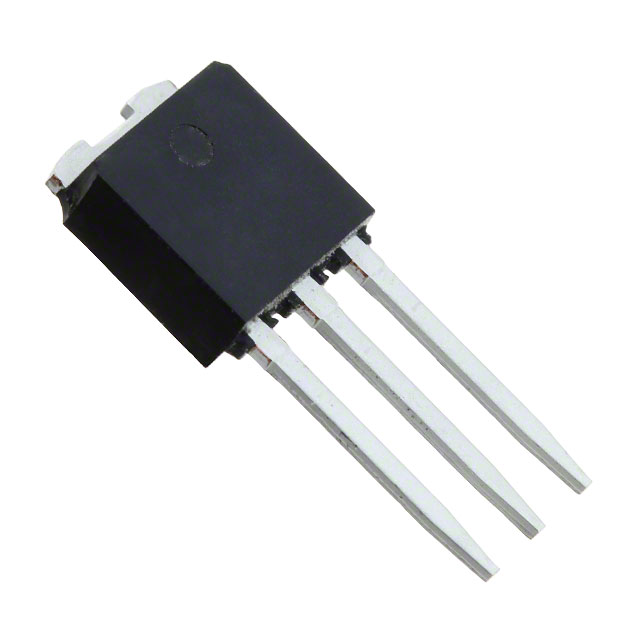
- Part No.:
- VND7N04-1
- Manufacturer:
- STMicroelectronics
- Package:
- TO-251-3 Short Leads, IPAK, TO-251AA
- Datasheet:
-
 VND7N04-1.pdf
- Description:
- IC PWR DRIVER N-CHANNEL 1:1 IPAK
- Quantity:
- Payment:

- Shipping:

Inventory:4,983
Please send an inquiry. Send us your inquiry, and we will respond immediately.
Product details
Overview
VND7N04-1 from STMicroelectronics is a monolithic VIPower M0 high-side smart power MOSFET designed for DC–50 kHz switching in automotive and industrial load control. It integrates linear current limiting (7 A), overvoltage clamp (42 V), thermal shutdown (150 °C), diagnostic feedback via input pin, and direct gate access for analog driving. Used in 12 V battery-fed solenoid, relay, and lamp drivers where fault resilience and compact integration are critical.
For engineers reviewing the VND7N04-1 datasheet, VND7N04-1 pinout, VND7N04-1 application, or VND7N04-1 equivalent, this page delivers verified electrical specs, protection behavior, package mapping to TO-252 (DPAK), real-world use cases, and validated alternative parts - all grounded in ST's official documentation (DocID4336 Rev 2).
Technical Context
The VND7N04-1 operates as a high-side switch with internal gate driver, current-sense, thermal sensor, and clamp circuitry. Its linear current limiter activates at 7 A (typ.) and holds ID constant regardless of input voltage, enabling predictable fault energy management. The integrated 42 V avalanche-rated clamp protects against inductive kickback without external components.
Fault detection is implemented via input pin voltage collapse: during overtemperature or short-circuit events, the input is actively pulled to ground through ~100 Ω, providing unambiguous status signaling. The device draws only 250–550 µA from the input pin under normal operation, supporting low-power logic-level drive.
Key Specifications
| Parameter | Value and Actual Design Meaning |
|---|---|
| VDS Clamp | 42 V - Rugged avalanche-rated clamping prevents destructive voltage spikes when switching inductive loads like solenoids or motors. |
| RDS(on) | 0.14 Ω @ Tj = 25 °C, VIN = 10 V - Enables <1 W conduction loss at 3.5 A, reducing heatsink requirements in space-constrained designs. |
| Ilim | 7 A - Precise linear current limit ensures consistent trip point across temperature and supply variations, simplifying system-level fault budgeting. |
| Tjsh / Tjrs | 150 °C shutdown / 135 °C reset - Hysteresis prevents thermal oscillation during overload recovery; enables self-recovery after transient faults. |
| VIN(th) | 0.8–3 V - TTL/CMOS-compatible input threshold allows direct interfacing with microcontrollers and logic ICs without level-shifting. |
| IISS | 250–550 µA - Ultra-low input supply current minimizes driver-stage loading and supports battery-powered or low-quiescent systems. |
| EAS | 0.4 J - Single-pulse avalanche energy rating validates robustness against unclamped inductive switching stress (e.g., relay coil de-energization). |
Pinout & Package
Package: TO-252 (DPAK), surface-mount, thermally enhanced with exposed drain pad for PCB heat sinking.
| Pin/Terminal | Circuit Role | Design Meaning |
|---|---|---|
| 1 (Source) | Power return path and substrate reference | Internally tied to chip ground; must be connected to system GND plane with low-inductance layout for stable protection response. |
| 2 (Drain) | Main power output terminal | Exposed metal pad on bottom of DPAK - electrically and thermally connected to internal MOSFET drain; requires soldered thermal pad to PCB copper pour. |
| 3 (Input) | Control and diagnostic interface | Drives internal gate; sinks fault current (~50 mA) during overtemperature/short-circuit; voltage drop signals fault condition to MCU GPIO. |
Key Features
| Feature | Design Value |
|---|---|
| Integrated overvoltage clamp | 42 V clamping with rugged avalanche capability eliminates need for external TVS or snubber networks in 12 V automotive applications. |
| Linear current limitation | 7 A regulated current limit maintains safe SOA during sustained overload, enabling predictable thermal design without external current sensing. |
| Thermal shutdown with hysteresis | 150 °C trip / 135 °C release provides reliable overtemperature protection with automatic recovery, avoiding latch-up behavior. |
| Diagnostic feedback via input pin | Active low fault signal (≈0 V via 100 Ω) enables real-time health monitoring using a single MCU GPIO-no additional sense resistors or comparators required. |
| Direct gate access | Analog-compatible input allows variable-duty-cycle PWM or linear regulation, supporting soft-start and current-controlled ramping for EMI reduction. |
Applications
| Automotive Body Control Module (BCM) | Industrial PLC Output Stage |
|---|---|
|
Use Scenario: Driving 12 V incandescent lamps and small solenoids in door lock actuators and interior lighting. IC Role / Device Role / Timing Role: High-side load switch with built-in diagnostics and short-circuit resilience. Use Value: Eliminates discrete protection components and enables per-channel fault reporting to BCM microcontroller via shared input pin. |
Use Scenario: Controlling 24 V DC solenoid valves and indicator lamps in factory automation I/O modules. IC Role / Device Role / Timing Role: Robust high-side driver with thermal and current fault detection for unattended operation. Use Value: Reduces board area by 40% vs discrete MOSFET + protection IC solution while improving reliability in dusty, high-temperature environments. |
| Motor Control Auxiliary Circuit | Smart Power Distribution Unit |
|
Use Scenario: Enabling/disabling auxiliary motor windings or brake coils in HVAC blower systems. IC Role / Device Role / Timing Role: Current-limited high-side switch with fast (<20 µs) step-response limiting for controlled inrush suppression. Use Value: Prevents nuisance tripping during motor startup while maintaining full 7 A capability for steady-state operation. |
Use Scenario: Providing individually protected 12 V outputs in vehicle infotainment power distribution boards. IC Role / Device Role / Timing Role: Smart power switch with integrated diagnostics and thermal management for multi-load systems. Use Value: Enables software-configurable load shedding and predictive maintenance based on cumulative fault event logging via input pin state. |
Equivalent & Alternatives
The following parts are listed as comparable options for similar high-side smart power switch applications.
| Alternative Part | Technical Difference | Application Difference | Selection Advice |
|---|---|---|---|
| VND7NV04 | Higher RDS(on) (0.25 Ω), same 42 V clamp and 7 A limit, but lower thermal performance (Rthj-case = 4.5 °C/W vs 3.75 °C/W). | Suitable for lower-current or less thermally constrained layouts; not recommended for continuous 3.5 A loads in sealed enclosures. | Select when cost sensitivity outweighs thermal margin, and PCB copper area for heat spreading is limited. |
| IPS1030H | Lower Ilim (3 A), higher VCLAMP (60 V), integrated current sense output (ISENSE), no analog gate drive capability. | Better suited for precision current monitoring applications; lacks linear driving mode and direct gate access. | Choose when accurate real-time current measurement is required, and 3 A max load current is sufficient. |
Compared with VND7N04-1, VND7NV04 trades thermal efficiency for cost, while IPS1030H shifts focus from analog controllability to digital current monitoring - making VND7N04-1 optimal for applications needing both robust fault handling and flexible analog/PWM drive.
Availability
VND7N04-1 is available at Aetrix Electronics and suitable for automotive body electronics, industrial PLC output stages, motor auxiliary circuits, and smart power distribution units requiring stable component supply and long-term lifecycle support.
Supply support for VND7N04-1 includes scheduled delivery planning, volume procurement assistance, BOM continuity management, traceable sourcing, and lifecycle availability coordination for OEM customers, industrial embedded developers, connected-device designers, and electronics production programs.
Manufacturer
STMicroelectronics is a global semiconductor leader headquartered in Geneva, Switzerland, specializing in automotive, industrial, and power management ICs with vertical manufacturing and broad IP portfolio.
The VND7N04-1 belongs to ST's OMNIFET family of VIPower high-side switches, engineered specifically for replacing discrete MOSFETs in harsh-environment load control where integrated protection, diagnostics, and compact packaging are essential.
FAQ
What is the maximum continuous drain current for VND7N04-1 under typical PCB thermal conditions?
The VND7N04-1 has a nominal current limit of 7 A, but continuous operation depends on PCB thermal design. With a standard 2-layer board and 200 mm² copper pour on the drain pad, derating begins above 3.5 A at ambient >60 °C. Full 7 A is sustainable only with forced air or large heatsink attachment per ST's Figure 3 derating curve.
Can VND7N04-1 be used in low-side switching configurations?
No - VND7N04-1 is strictly a high-side switch. Its source terminal is internally tied to ground reference, and the input pin controls the gate relative to source. Low-side operation would reverse internal protection logic and disable fault feedback; it is not rated or characterized for that topology.
How does the diagnostic feedback signal behave during a short-circuit event?
During short-circuit, the input pin is actively pulled to ground through an internal ~100 Ω resistor, dropping its voltage to <0.5 V. This occurs within 13–25 µs (depending on input voltage), and persists until junction temperature falls below 135 °C. No external pull-up is needed - the MCU reads this as a logic-low fault flag.
Is VND7N04-1 qualified for automotive applications per AEC-Q100?
No - ST's official documentation (DocID4336 Rev 2) states VND7N04-1 is not designed or authorized for automotive safety-critical or AEC-Q100 qualified applications. It is intended for industrial and general-purpose load control; automotive-grade equivalents include the AEC-Q100 qualified VNQ7E050AK.
VND7N04-1 Specifications
- Product attributes
- Attribute value
- Manufacturer:
- STMicroelectronics
- Package/Case:
- TO-251-3 Short Leads, IPAK, TO-251AA
- Series:
- OMNIFET II™, VIPower™
- Packaging:
- Tube
- Product Status:
- Obsolete
- Switch Type:
- General Purpose
- Number of Outputs:
- 1
- Ratio - Input:Output:
- 1:1
- Output Configuration:
- Low Side
- Output Type:
- N-Channel
- Interface:
- On/Off
- Voltage - Load:
- 31V (Max)
- Voltage - Supply (Vcc/Vdd):
- Not Required
- Current - Output (Max):
- 4A
- Rds On (Typ):
- 140mOhm (Max)
- Input Type:
- Non-Inverting
- Features:
- -
- Fault Protection:
- Current Limiting (Fixed), Over Temperature, Over Voltage
- Operating Temperature:
- -40°C ~ 150°C (TJ)
- Grade:
- -
- Qualification:
- -
- Mounting Type:
- Through Hole
- Supplier Device Package:
- IPAK
VND7N04-1 FAQ
1.How can I place an order for VND7N04-1 through Aetrix?
Please submit a Request for Quotation (RFQ) for VND7N04-1 on Aetrix. Our sales agent will provide a competitive quotation and guide you through the order confirmation once you accept the terms.
2.Are the price and stock information for VND7N04-1 reliable?
The price and inventory of VND7N04-1 are updated periodically and may fluctuate due to market conditions. Stock and pricing data are typically refreshed every 24 hours. Quotation validity for VND7N04-1 is usually 5 days.
3.What payment methods are accepted for VND7N04-1?
We accept Wire Transfer, PayPal, Credit Card, Western Union, MoneyGram, and Escrow for VND7N04-1 transactions.
Note: Certain payment methods may incur a processing fee.
4.How is shipping managed for VND7N04-1?
VND7N04-1 orders can be shipped via leading logistics carriers, including DHL, UPS, FedEx, TNT, or Registered Mail.
Once your VND7N04-1 order is processed, you will receive an email with the shipment details and tracking number.
Note: Tracking information may take up to 24 hours to appear. Express delivery typically takes 3–5 business days.
5.How can I obtain technical support or documentation for VND7N04-1?
For technical support, including VND7N04-1 datasheets, pinout diagrams, or application guidance, please contact our engineering support team. They can provide detailed documentation and assistance for your VND7N04-1 requirements.
6.How does Aetrix verify that VND7N04-1 is sourced from the original manufacturer or authorized distributors?
All VND7N04-1 products on Aetrix are procured from qualified distributors and authorized channels. Our dedicated quality assurance team conducts strict verification, including traceability checks and, if necessary, third-party testing. This ensures that VND7N04-1 meets industry standards.
7.What is the process for return or replacement of VND7N04-1?
All VND7N04-1 units undergo pre-shipment inspection (PSI). If there is an issue with VND7N04-1, returns or replacements are accepted under the following conditions:
1.Quantity discrepancies, incorrect items, or visible external defects (such as breakage or corrosion), acknowledged by Aetrix.
2.The issue is reported within 90 days of delivery.
3.The VND7N04-1 part is unused and in its original packaging.
Return procedure for VND7N04-1:
1.Submit a request within 90 days.
2.Obtain a Return Material Authorization (RMA) from Aetrix.
VND7N04-1 Tags

-
TPS22919DCKR
Texas Instruments

-
MIC2091-1YM5-TR
Microchip Technology

-
MIC2090-1YM5-TR
Microchip Technology

-
TPS22995RZFR
Texas Instruments

-
TPS22975DSGR
Texas Instruments

-
SIP32510DT-T1-GE3
Vishay Siliconix

-
ULN2003D1013TR
STMicroelectronics

-
MIC2005A-1YM5-TR
Microchip Technology

-
MIC2005A-1YM6-TR
Microchip Technology

-
TPS22916BYFPR
Texas Instruments

-
TPS22917DBVR
Texas Instruments

-
ULN2003APWR
Texas Instruments
Tech Hub

A practical engineering and sourcing framework covering lifecycle verification, lifetime-buy calculations, replacement qualification, supplier checks and counterfeit-risk controls.

TTL and CMOS logic families differ in thresholds, loading, output drive, power and timing. This engineering guide compares 74HC and 74HCT, calculates noise margins and checks 3.3 V/5 V compatibility.

A practical engineering guide to 3.3V and 5V logic compatibility, input thresholds, resistor dividers, translator ICs, MOSFET level shifting, I2C pull-ups, timing limits and power-sequencing risks.

The 74HC595 uses push-pull logic outputs, while the TPIC6B595 uses 50 V open-drain DMOS sinks for higher-power loads. This guide compares timing, current limits, 3.3 V interfacing, load wiring, thermal…

The 74HC595 converts serial data into eight stable parallel outputs. This guide covers pin functions, shift and storage timing, OE and MR behavior, drive-current limits, cascading, voltage compatibilit…

A technical comparison of level-sensitive latches and edge-triggered flip-flops, covering timing windows, setup and hold limits, master–slave operation, time borrowing, race-through, HDL inference and…

A D latch stores one bit while Enable controls when data can pass. This reference covers gate-level operation, truth tables, transparency, setup and hold timing, LE versus OE, common ICs and practical …

An SR latch stores one bit through cross-coupled feedback. This engineering reference covers NOR and NAND implementations, truth tables, forbidden-state recovery, gated operation, switch debouncing, fa…

Latch circuits retain one bit through feedback. This technical reference covers SR and D latches, truth tables, transparency, timing limits, latch-versus-flip-flop behavior, applications and common log…

An engineering guide to LED driver operation, constant-current and constant-voltage outputs, linear and switching topologies, dimming, IC selection, calculations, replacement compatibility, and fault c…


