
 My Inquiry
 My Account


STMicroelectronics VNN3NV04PTR-E
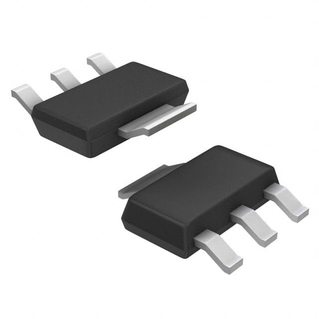
- Part No.:
- VNN3NV04PTR-E
- Manufacturer:
- STMicroelectronics
- Package:
- TO-261-4, TO-261AA
- Datasheet:
-
 VNN3NV04PTR-E.pdf
- Description:
- IC PWR DRIVER N-CHAN 1:1 SOT223
- Quantity:
- Payment:

- Shipping:

Inventory:3,334
Please send an inquiry. Send us your inquiry, and we will respond immediately.
Product details
Overview
VNN3NV04PTR-E from STMicroelectronics is a monolithic OMNIFET II fully autoprotected Power MOSFET in SOT-223 package, designed as a rugged replacement for standard N-channel Power MOSFETs in DC–50 kHz switching applications. It features 120 mΩ RDS(on), 3.5 A linear current limit, and integrated 40 V overvoltage clamp - enabling reliable load switching in automotive body electronics, industrial I/O modules, and 24 V DC power distribution systems.
For engineers reviewing the VNN3NV04PTR-E datasheet, VNN3NV04PTR-E pinout, VNN3NV04PTR-E application, or VNN3NV04PTR-E equivalent, key selection criteria include its diagnostic feedback via input pin, thermal shutdown at 170 °C typical, direct gate access for analog driving, ESD robustness (4 kV HBM), and compatibility with TTL-level logic drive.
Technical Context
This device integrates VIPower® M0-3 technology to embed protection circuitry directly into the power stage: linear current limiting operates independently of input voltage, while overtemperature sensing occurs locally in the power die region for fast response. The internal clamp diode and avalanche-rated structure support unclamped inductive switching up to 100 mJ single-pulse energy.
Operation relies on low-impedance gate connection - input pin drives the MOSFET gate directly, drawing only 100–150 µA supply current during normal conduction. Fault detection is implemented by sinking 10–20 mA diagnostic current (Igf) into the input pin when junction temperature exceeds 170 °C, enabling system-level fault signaling without external sensors.
Key Specifications
| Parameter | Value and Actual Design Meaning |
|---|---|
| RDS(on) | 120 mΩ @ VIN = 5 V, ID = 1.5 A, Tj = 25 °C - enables low-conduction-loss switching in 24 V loads up to ~3 A continuous. |
| Ilim | 3.5 A min @ VIN = 5 V, VDS = 13 V - provides predictable current limiting during overload or short-circuit events. |
| VCLAMP | 40 V typ @ ID = 1.5 A - clamps inductive kickback to protect downstream circuitry without external snubbers. |
| Tjsh | 150–200 °C shutdown range, 170 °C typical - triggers thermal cutoff before silicon damage, with 15 °C hysteresis for auto-restart. |
| Igf | 10–20 mA fault sink current - allows direct interface with microcontroller GPIO for hardware-level fault reporting. |
| ESD Rating | 4000 V HBM (R = 1.5 kΩ, C = 100 pF) - meets automotive and industrial ESD immunity requirements without external protection. |
| Switching Speed | td(on) = 90 ns, tr = 250 ns @ Rgen = 220 Ω - supports clean turn-on in high-frequency DC-DC and PWM motor control. |
Pinout & Package
SOT-223 package: surface-mount, thermally enhanced 4-pin outline with exposed drain pad (pin 2) for improved heat dissipation. Pin 1 = INPUT, Pin 2 = DRAIN (connected to tab), Pin 3 = SOURCE, Pin 4 = SOURCE (dual-source configuration).
| Pin/Terminal | Circuit Role | Design Meaning |
|---|---|---|
| Pin 1 (INPUT) | Gate control & fault feedback node | Directly drives internal MOSFET gate; sinks 10–20 mA diagnostic current during thermal fault - requires ≥220 Ω series impedance for safe operation. |
| Pin 2 (DRAIN) | Main power output terminal | Connected to exposed metal tab; carries full load current and dissipates heat - must be soldered to large copper pour for Rthj-case ≤ 18 °C/W. |
| Pins 3 & 4 (SOURCE) | Power return and reference ground | Dual-source configuration reduces source inductance; establishes local ground reference for current-sense and protection circuits. |
Key Features
| Feature | Design Value |
|---|---|
| Linear current limitation | Clamps ID to 3.5 A regardless of VIN; avoids destructive latch-up during sustained overload. |
| Integrated overvoltage clamp | 40 V threshold with rugged avalanche capability - eliminates need for external TVS or Zener clamping in solenoid/relay drivers. |
| Thermal shutdown with hysteresis | Shuts down at 170 °C typical, restarts at ~155 °C - prevents thermal runaway in sealed enclosures or poor airflow conditions. |
| Diagnostic feedback via input pin | Sinks 15 mA fault current into INPUT pin - enables direct GPIO monitoring without optocouplers or ADC channels. |
| Direct gate access (analog driving) | Input pin connects directly to gate with no internal level-shifter - supports variable-duty PWM and linear regulation modes. |
Applications
| Automotive Body Control Module | Industrial PLC Output Stage |
|---|---|
|
Use Scenario: Driving 12 V/24 V solenoids, door locks, and HVAC actuators in vehicle body electronics. IC Role / Device Role: High-side load switch with built-in short-circuit and overtemperature protection. Use Value: Eliminates need for discrete current sense, thermal sensor, and clamp diode - reduces BOM count by 4 components per channel. |
Use Scenario: Solid-state replacement for electromechanical relays in programmable logic controller digital outputs. IC Role / Device Role: Protected low-side switching element for 24 V DC field devices (valves, indicators, sensors). Use Value: Supports >100,000 switching cycles with no contact wear; withstands 107 ns reverse recovery time during inductive turn-off. |
| Smart Lighting Power Distribution | Medical Equipment Power Sequencing |
|
Use Scenario: Individual channel control for LED string drivers and emergency lighting systems in commercial buildings. IC Role / Device Role: Current-limited, thermally protected power switch for constant-current LED loads. Use Value: Maintains stable 3.5 A current limit across -40 °C to +150 °C ambient - ensures consistent brightness and safety certification compliance. |
Use Scenario: Controlled power-up sequencing of isolated subsystems in diagnostic imaging and patient monitors. IC Role / Device Role: Fault-isolated power enable switch with diagnostic feedback for safety-critical power rails. Use Value: Provides hardware-level fault indication (Igf sink) that satisfies IEC 62304 Class C software independence requirements. |
Equivalent & Alternatives
The following parts are listed as comparable options for similar protected Power MOSFET applications.
| Alternative Part | Technical Difference | Application Difference | Selection Advice |
|---|---|---|---|
| STP36NF06L | Standard N-channel MOSFET, no integrated protection; RDS(on) = 40 mΩ @ 10 V, but requires external current sense, thermal monitor, and clamp. | Lacks fault feedback, linear current limit, and thermal shutdown - suitable only where protection is implemented at system level. | Select when cost sensitivity outweighs design simplicity and board space constraints. |
| VND5T016AKTR-E | Higher voltage rating (45 V), dual-channel, 160 mΩ RDS(on), same VIPower M0-3 architecture and diagnostic feedback capability. | Designed for dual-load applications (e.g., mirror/heater control); shares identical protection behavior but higher on-resistance. | Choose for space-constrained dual-output designs requiring matched protection features and footprint compatibility. |
Compared with STP36NF06L, VNN3NV04PTR-E trades 80 mΩ higher RDS(on) for autonomous protection and diagnostics; versus VND5T016AKTR-E, it offers lower on-resistance and single-channel optimization for cost-sensitive single-load systems.
Availability
VNN3NV04PTR-E is available at Aetrix Electronics and suitable for automotive body electronics, industrial PLC output stages, and smart lighting power distribution requiring stable component supply and long-term production continuity.
Supply support for VNN3NV04PTR-E includes scheduled delivery planning, volume procurement assistance, BOM continuity management, traceable sourcing, and lifecycle availability coordination for OEM customers, industrial embedded developers, connected-device designers, and electronics production programs.
Manufacturer
STMicroelectronics is a global semiconductor leader headquartered in Geneva, Switzerland, specializing in power management, automotive ICs, and embedded processing solutions.
VNN3NV04PTR-E belongs to the OMNIFET II family of protected Power MOSFETs, engineered specifically for replacing mechanical relays and unprotected discrete switches in harsh industrial and automotive environments.
FAQ
What is the maximum continuous drain current for VNN3NV04PTR-E under typical PCB conditions?
The device delivers 3.5 A continuous drain current with linear current limiting active. At Tc = 25 °C on a standard FR4 board with 50 mm² copper pour, its 7 W total dissipation supports ~2.5 A continuous conduction before thermal derating begins - confirmed by Figure 10 derating curve in ST's Doc ID 15626 Rev. 5.
Can VNN3NV04PTR-E be used in high-side switching configurations?
No - VNN3NV04PTR-E is a low-side N-channel switch with SOURCE pins referenced to system ground. Its INPUT pin controls the gate relative to SOURCE, making it unsuitable for high-side use without level-shifting circuitry. For high-side applications, ST recommends VNH5019AS or similar integrated half-bridges.
How does the diagnostic feedback mechanism work during thermal fault?
When junction temperature exceeds 170 °C, the device sinks 10–20 mA (Igf) into the INPUT pin. If driven by a low-impedance source (e.g., MCU GPIO with 220 Ω series resistor), this pulls the input voltage toward 0 V, signaling fault. No external pull-up is required - the behavior is self-contained and electrically defined in Table 4.
Is the SOT-223 package RoHS-compliant and lead-free?
Yes - VNN3NV04PTR-E uses ST's ECOPACK®-compliant SOT-223 package, meeting RoHS Directive 2011/65/EU and REACH regulations. The "TR" suffix denotes tape-and-reel packaging with lead-free matte tin plating, verified per ST's official product change notification PCN-2012-018.
VNN3NV04PTR-E Specifications
- Product attributes
- Attribute value
- Manufacturer:
- STMicroelectronics
- Package/Case:
- TO-261-4, TO-261AA
- Series:
- OMNIFET II™, VIPower™
- Packaging:
- Tape & Reel (TR)
- Product Status:
- Active
- Switch Type:
- General Purpose
- Number of Outputs:
- 1
- Ratio - Input:Output:
- 1:1
- Output Configuration:
- Low Side
- Output Type:
- N-Channel
- Interface:
- On/Off
- Voltage - Load:
- 36V (Max)
- Voltage - Supply (Vcc/Vdd):
- Not Required
- Current - Output (Max):
- 3.5A
- Rds On (Typ):
- 120mOhm (Max)
- Input Type:
- Non-Inverting
- Features:
- -
- Fault Protection:
- Current Limiting (Fixed), Over Temperature, Over Voltage
- Operating Temperature:
- -40°C ~ 150°C (TJ)
- Grade:
- -
- Qualification:
- -
- Mounting Type:
- Surface Mount
- Supplier Device Package:
- SOT-223
VNN3NV04PTR-E FAQ
1.How can I place an order for VNN3NV04PTR-E through Aetrix?
Please submit a Request for Quotation (RFQ) for VNN3NV04PTR-E on Aetrix. Our sales agent will provide a competitive quotation and guide you through the order confirmation once you accept the terms.
2.Are the price and stock information for VNN3NV04PTR-E reliable?
The price and inventory of VNN3NV04PTR-E are updated periodically and may fluctuate due to market conditions. Stock and pricing data are typically refreshed every 24 hours. Quotation validity for VNN3NV04PTR-E is usually 5 days.
3.What payment methods are accepted for VNN3NV04PTR-E?
We accept Wire Transfer, PayPal, Credit Card, Western Union, MoneyGram, and Escrow for VNN3NV04PTR-E transactions.
Note: Certain payment methods may incur a processing fee.
4.How is shipping managed for VNN3NV04PTR-E?
VNN3NV04PTR-E orders can be shipped via leading logistics carriers, including DHL, UPS, FedEx, TNT, or Registered Mail.
Once your VNN3NV04PTR-E order is processed, you will receive an email with the shipment details and tracking number.
Note: Tracking information may take up to 24 hours to appear. Express delivery typically takes 3–5 business days.
5.How can I obtain technical support or documentation for VNN3NV04PTR-E?
For technical support, including VNN3NV04PTR-E datasheets, pinout diagrams, or application guidance, please contact our engineering support team. They can provide detailed documentation and assistance for your VNN3NV04PTR-E requirements.
6.How does Aetrix verify that VNN3NV04PTR-E is sourced from the original manufacturer or authorized distributors?
All VNN3NV04PTR-E products on Aetrix are procured from qualified distributors and authorized channels. Our dedicated quality assurance team conducts strict verification, including traceability checks and, if necessary, third-party testing. This ensures that VNN3NV04PTR-E meets industry standards.
7.What is the process for return or replacement of VNN3NV04PTR-E?
All VNN3NV04PTR-E units undergo pre-shipment inspection (PSI). If there is an issue with VNN3NV04PTR-E, returns or replacements are accepted under the following conditions:
1.Quantity discrepancies, incorrect items, or visible external defects (such as breakage or corrosion), acknowledged by Aetrix.
2.The issue is reported within 90 days of delivery.
3.The VNN3NV04PTR-E part is unused and in its original packaging.
Return procedure for VNN3NV04PTR-E:
1.Submit a request within 90 days.
2.Obtain a Return Material Authorization (RMA) from Aetrix.
VNN3NV04PTR-E Tags

-
TPS22919DCKR
Texas Instruments

-
MIC2091-1YM5-TR
Microchip Technology

-
MIC2090-1YM5-TR
Microchip Technology

-
TPS22995RZFR
Texas Instruments

-
TPS22975DSGR
Texas Instruments

-
SIP32510DT-T1-GE3
Vishay Siliconix

-
ULN2003D1013TR
STMicroelectronics

-
MIC2005A-1YM5-TR
Microchip Technology

-
MIC2005A-1YM6-TR
Microchip Technology

-
TPS22916BYFPR
Texas Instruments

-
TPS22917DBVR
Texas Instruments

-
ULN2003APWR
Texas Instruments
Tech Hub

A practical engineering and sourcing framework covering lifecycle verification, lifetime-buy calculations, replacement qualification, supplier checks and counterfeit-risk controls.

TTL and CMOS logic families differ in thresholds, loading, output drive, power and timing. This engineering guide compares 74HC and 74HCT, calculates noise margins and checks 3.3 V/5 V compatibility.

A practical engineering guide to 3.3V and 5V logic compatibility, input thresholds, resistor dividers, translator ICs, MOSFET level shifting, I2C pull-ups, timing limits and power-sequencing risks.

The 74HC595 uses push-pull logic outputs, while the TPIC6B595 uses 50 V open-drain DMOS sinks for higher-power loads. This guide compares timing, current limits, 3.3 V interfacing, load wiring, thermal…

The 74HC595 converts serial data into eight stable parallel outputs. This guide covers pin functions, shift and storage timing, OE and MR behavior, drive-current limits, cascading, voltage compatibilit…

A technical comparison of level-sensitive latches and edge-triggered flip-flops, covering timing windows, setup and hold limits, master–slave operation, time borrowing, race-through, HDL inference and…

A D latch stores one bit while Enable controls when data can pass. This reference covers gate-level operation, truth tables, transparency, setup and hold timing, LE versus OE, common ICs and practical …

An SR latch stores one bit through cross-coupled feedback. This engineering reference covers NOR and NAND implementations, truth tables, forbidden-state recovery, gated operation, switch debouncing, fa…

Latch circuits retain one bit through feedback. This technical reference covers SR and D latches, truth tables, transparency, timing limits, latch-versus-flip-flop behavior, applications and common log…

An engineering guide to LED driver operation, constant-current and constant-voltage outputs, linear and switching topologies, dimming, IC selection, calculations, replacement compatibility, and fault c…


