
 My Inquiry
 My Account


Vishay Semiconductor Opto Division VOR2142B8T
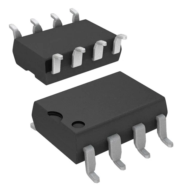
- Part No.:
- VOR2142B8T
- Manufacturer:
- Vishay Semiconductor Opto Division
- Category:
- Solid State Relays (SSR)
- Package:
- 8-SMD (0.300", 7.62mm)
- Datasheet:
-
 VOR2142B8T.pdf
- Description:
- SSR RELAY SPST-NO 140MA 0-400V
- Quantity:
- Payment:

- Shipping:

Inventory:993
Please send an inquiry. Send us your inquiry, and we will respond immediately.
Product details
Overview
VOR2142B8T from Vishay Semiconductors is a dual-channel, normally open, optically isolated solid-state relay (SPST, 1 Form A) with 400 V load voltage rating, 140 mA single-channel DC load current, and 22 Ω typical on-resistance. It uses a GaAlAs IRED input and high-performance MOSFET output switches to enable clean, bounce-free AC/DC switching in telecom, metering, and industrial control systems.
For engineers reviewing the VOR2142B8T datasheet, VOR2142B8T pinout, VOR2142B8T application, or VOR2142B8T equivalent, this device delivers verified 5300 VRMS isolation, sub-500 µs turn-on/turn-off times, and SMD-8 packaging suitable for automated assembly in space-constrained, safety-critical signal routing designs.
Technical Context
The VOR2142B8T implements hybrid optocoupler architecture: an infrared LED drives two independent photodetector-MOSFET output stages, each with integrated gate drive and protection circuitry. Its dual-channel layout supports independent control of two isolated loads without crosstalk.
It operates across -40 °C to +100 °C ambient temperature, maintains ≤27 Ω RON up to 100 °C, and sustains 400 V peak load voltage with <500 nA off-state leakage at rated voltage - meeting UL 1577 and DIN EN 60747-5-5 (VDE 0884-5) safety standards.
Key Specifications
| Parameter | Value and Actual Design Meaning |
|---|---|
| Isolation Voltage | 5300 VRMS - enables reinforced insulation per UL/cUL/VDE for mains-connected equipment |
| Load Voltage Rating | 400 V - supports direct switching of 230 VAC RMS and 350 VDC bus lines |
| Max Load Current | 140 mA (one channel), 100 mA (both channels) - defines simultaneous switching capacity under thermal derating |
| On-Resistance | 22 Ω typical - limits power loss to ≤220 mW at 100 mA, enabling low-self-heating operation |
| Switching Speed | 0.13 ms turn-on / 0.05 ms turn-off - ensures precise timing control in ATE and fast-response security circuits |
| Input Forward Current | 0.25 mA typical for turn-on - allows direct drive from low-power MCU GPIOs without external amplification |
| Ambient Temp Range | -40 °C to +100 °C - supports deployment in uncooled industrial enclosures and outdoor metering housings |
Pinout & Package
SMD-8 surface-mount package with 2.54 mm lead pitch, 9.80 mm × 6.65 mm body, and 0.79 mm nominal height; creepage/clearance ≥8 mm meets reinforced insulation requirements.
| Pin/Terminal | Circuit Role | Design Meaning |
|---|---|---|
| 1, 2 | Channel 1 IRED Anode/Cathode | Optically couples to Output 1; requires series resistor for IF ≤50 mA |
| 3, 4 | Channel 2 IRED Anode/Cathode | Independent optical input for Output 2; electrically isolated from Channel 1 |
| 5, 6 | Channel 1 Load Terminals (S1, S1′) | SPST switch contacts rated 400 V/140 mA; bidirectional AC/DC conduction |
| 7, 8 | Channel 2 Load Terminals (S2, S2′) | Second isolated SPST path; no shared terminals with Channel 1 |
Key Features
| Feature | Design Value |
|---|---|
| Dual independent SSR channels | Enables compact replacement of two discrete mechanical relays or opto-TRIACs in space-limited PCB layouts |
| 5300 VRMS isolation | Meets reinforced insulation requirements for functional safety in Class I equipment without additional barrier design |
| Clean bounce-free switching | Eliminates contact arcing and EMI in precision instrumentation and battery management sampling circuits |
| Low 0.25 mA turn-on IF | Reduces system-level power consumption and simplifies drive circuitry versus legacy optorelays |
| Wide -40 °C to +100 °C operation | Supports deployment in automotive under-hood modules and industrial PLC backplanes without derating |
Applications
| Telecom Line Switching | Metering Input Isolation |
|---|---|
Use Scenario: Routing analog voice/data signals between line cards and test ports in PSTN access nodes. IC Role / Device Role / Timing Role: Dual-channel optically isolated SPST switch providing galvanic separation between subscriber lines and central office logic. Use Value: Prevents ground loop noise and fault propagation while supporting 400 V transient immunity on tip/ring pairs. |
Use Scenario: Isolating voltage/current sensing inputs in smart electricity meters exposed to 230 VAC mains. IC Role / Device Role / Timing Role: Solid-state relay decoupling measurement front-end from microcontroller ADC reference domain. Use Value: Maintains ±0.1% measurement accuracy by eliminating leakage-induced offset drift across 10+ year field life. |
| Security Panel Zone Control | Industrial PLC Output Module |
Use Scenario: Supervising door/window sensor loops in fire alarm and intrusion detection panels. IC Role / Device Role / Timing Role: Optically isolated switch enabling supervised zone monitoring with end-of-line resistor detection. Use Value: Provides fail-safe open/short detection without mechanical contact wear or false alarms from vibration. |
Use Scenario: Driving solenoid valves and indicator lamps in modular industrial control cabinets. IC Role / Device Role / Timing Role: Dual-channel SSR replacing electromechanical relays to eliminate coil drive complexity and contact bounce. Use Value: Achieves >10⁷ operations lifetime and 100 µs response time for closed-loop motion control sequencing. |
Equivalent & Alternatives
The following parts are listed as comparable options for similar solid-state relay applications.
| Alternative Part | Technical Difference | Application Difference | Selection Advice |
|---|---|---|---|
| TLP3548A | Single-channel, 60 V load rating, 2.5 A load current, SO-6 package | Higher current, lower voltage; unsuitable for 230 VAC metering or telecom line isolation | Select when driving high-current DC loads below 60 V with minimal board area |
| PS7142-2A | Dual-channel, 400 V rating, but 100 mA max load current and 35 Ω typical RON in DIP-8 | Same voltage class but higher on-resistance and larger footprint; lacks SMD-8 tape-and-reel option | Choose only if DIP-8 through-hole assembly is required and thermal budget allows higher I²R loss |
Compared with TLP3548A and PS7142-2A, the VOR2142B8T uniquely balances dual-channel 400 V capability, SMD-8 manufacturability, and 22 Ω RON - making it optimal for high-density, safety-certified AC/DC switching where both channels must handle 140 mA at minimal self-heating.
Availability
VOR2142B8T is available at Aetrix Electronics and suitable for telecom switching, smart metering, security equipment, and industrial controls requiring stable component supply, long-term lifecycle support, and traceable sourcing.
Supply support for VOR2142B8T includes scheduled delivery planning, volume procurement assistance, BOM continuity management, traceable sourcing, and lifecycle availability coordination for OEM customers, industrial embedded developers, connected-device designers, and electronics production programs.
Manufacturer
Vishay Intertechnology is a global semiconductor manufacturer specializing in discrete components, sensors, and optoelectronics with emphasis on reliability, safety certification, and high-voltage isolation performance.
The VOR2142 series is part of Vishay's optically isolated solid-state relay product line, engineered specifically for replacing electromechanical relays in safety-critical AC/DC signal routing applications demanding long service life and zero contact wear.
FAQ
What is the maximum continuous load current per channel for VOR2142B8T at 85 °C ambient?
The VOR2142B8T supports 140 mA continuous DC load current per channel at 25 °C, but derates to approximately 100 mA per channel at 85 °C ambient temperature as shown in Figure 4 of the datasheet. This derating ensures junction temperature remains within the 125 °C limit under worst-case power dissipation conditions. The VOR2142B8T must be used with appropriate PCB copper area or thermal vias when operating near its thermal limits.
Does VOR2142B8T support AC load switching, and what is its zero-crossing behavior?
The VOR2142B8T supports both AC and DC load switching due to its back-to-back MOSFET output configuration, but it does not include zero-crossing detection circuitry. Switching occurs immediately upon input activation, resulting in non-zero-crossing turn-on. This enables precise timing control in ATE applications but may generate higher EMI during AC switching compared to zero-crossing TRIAC-based optocouplers. The VOR2142B8T is specified for clean bounce-free operation regardless of load type.
What is the minimum forward current required to reliably turn on VOR2142B8T at -40 °C?
At -40 °C, the VOR2142B8T requires a minimum forward current of approximately 0.35 mA to ensure reliable turn-on, based on the normalized forward current curve in Figure 7 of the datasheet. This represents a ~40 % increase over the 0.25 mA typical value at 25 °C. Designers should verify drive capability across the full temperature range, especially when using weak GPIO sources. The VOR2142B8T maintains guaranteed turn-on down to this level without external biasing.
Can VOR2142B8T replace mechanical relays in battery management system contactor control?
The VOR2142B8T is suitable for low-side precharge and auxiliary signal routing in BMS architectures, but not for main contactor switching due to its 140 mA load current limit and 400 V blocking rating. It can isolate voltage sense lines, thermistor inputs, or cell balancing enable signals where galvanic separation and bounce-free operation are critical. For main contactor control, higher-current SSRs or contactors remain necessary. The VOR2142B8T provides certified isolation and long-term reliability for these secondary BMS functions.
What safety certifications does VOR2142B8T hold, and what do they cover?
The VOR2142B8T is certified to UL 1577 (5300 VRMS, 1 min), cUL, and DIN EN 60747-5-5 (VDE 0884-5) for reinforced insulation. These approvals cover input-to-output withstand voltage, partial discharge limits, creepage/clearance distances (≥8 mm for SMD-8), and material tracking index (CTI = 175). The certifications apply to the full operating temperature range (-40 °C to +100 °C) and validate safe electrical insulation for use in double-insulated equipment. The VOR2142B8T meets the requirements for "safe electrical insulation" as defined in IEC 60747-5-5 §7.4.3.8.2.
VOR2142B8T Specifications
- Product attributes
- Attribute value
- Manufacturer:
- Vishay Semiconductor Opto Division
- Series:
- VOR2142
- Packaging:
- Tape & Reel (TR)
- Product Status:
- Active
- Mounting Type:
- Surface Mount
- Circuit:
- SPST-NO (1 Form A) x 2
- Output Type:
- AC, DC
- Voltage - Input:
- 1.36VDC
- Voltage - Load:
- 0 V ~ 400 V
- Load Current:
- 140 mA
- On-State Resistance (Max):
- 27 Ohms
- Termination Style:
- Gull Wing
- Operating Temperature:
- -40°C ~ 100°C
- Supplier Device Package:
- 8-SMD
- Approval Agency:
- cUL, DIN, UL
- Grade:
- -
- Qualification:
- -
VOR2142B8T FAQ
1.How can I place an order for VOR2142B8T through Aetrix?
Please submit a Request for Quotation (RFQ) for VOR2142B8T on Aetrix. Our sales agent will provide a competitive quotation and guide you through the order confirmation once you accept the terms.
2.Are the price and stock information for VOR2142B8T reliable?
The price and inventory of VOR2142B8T are updated periodically and may fluctuate due to market conditions. Stock and pricing data are typically refreshed every 24 hours. Quotation validity for VOR2142B8T is usually 5 days.
3.What payment methods are accepted for VOR2142B8T?
We accept Wire Transfer, PayPal, Credit Card, Western Union, MoneyGram, and Escrow for VOR2142B8T transactions.
Note: Certain payment methods may incur a processing fee.
4.How is shipping managed for VOR2142B8T?
VOR2142B8T orders can be shipped via leading logistics carriers, including DHL, UPS, FedEx, TNT, or Registered Mail.
Once your VOR2142B8T order is processed, you will receive an email with the shipment details and tracking number.
Note: Tracking information may take up to 24 hours to appear. Express delivery typically takes 3–5 business days.
5.How can I obtain technical support or documentation for VOR2142B8T?
For technical support, including VOR2142B8T datasheets, pinout diagrams, or application guidance, please contact our engineering support team. They can provide detailed documentation and assistance for your VOR2142B8T requirements.
6.How does Aetrix verify that VOR2142B8T is sourced from the original manufacturer or authorized distributors?
All VOR2142B8T products on Aetrix are procured from qualified distributors and authorized channels. Our dedicated quality assurance team conducts strict verification, including traceability checks and, if necessary, third-party testing. This ensures that VOR2142B8T meets industry standards.
7.What is the process for return or replacement of VOR2142B8T?
All VOR2142B8T units undergo pre-shipment inspection (PSI). If there is an issue with VOR2142B8T, returns or replacements are accepted under the following conditions:
1.Quantity discrepancies, incorrect items, or visible external defects (such as breakage or corrosion), acknowledged by Aetrix.
2.The issue is reported within 90 days of delivery.
3.The VOR2142B8T part is unused and in its original packaging.
Return procedure for VOR2142B8T:
1.Submit a request within 90 days.
2.Obtain a Return Material Authorization (RMA) from Aetrix.
VOR2142B8T Tags
.jpg)
-
G3VM-21UR11(TR05)
Omron Electronics Inc-EMC Div
-
G3VM-61VY3(TR05)
Omron Electronics Inc-EMC Div
-
CPC1017NTR
Littelfuse Inc.
-
CPC1017N
Littelfuse Inc.
-
CPC1006N
Littelfuse Inc.
-
VO1400AEFTR
Vishay Semiconductor Opto Division
-
CPC1006NTR
Littelfuse Inc.
-
TLP175A(TPL,E
Toshiba Semiconductor and Storage
-
CPC1002NTR
Littelfuse Inc.
-
AQY280S
Panasonic Electric Works
-
CPC1117NTR
Littelfuse Inc.
-
CPC1106NTR
Littelfuse Inc.
Tech Hub

Counterfeit components can hide behind convincing markings and passing basic function tests. This engineering reference covers source traceability, external inspection, X-ray, XRF, electrical testing, …

A practical engineering and sourcing framework covering lifecycle verification, lifetime-buy calculations, replacement qualification, supplier checks and counterfeit-risk controls.

TTL and CMOS logic families differ in thresholds, loading, output drive, power and timing. This engineering guide compares 74HC and 74HCT, calculates noise margins and checks 3.3 V/5 V compatibility.

A practical engineering guide to 3.3V and 5V logic compatibility, input thresholds, resistor dividers, translator ICs, MOSFET level shifting, I2C pull-ups, timing limits and power-sequencing risks.

The 74HC595 uses push-pull logic outputs, while the TPIC6B595 uses 50 V open-drain DMOS sinks for higher-power loads. This guide compares timing, current limits, 3.3 V interfacing, load wiring, thermal…

The 74HC595 converts serial data into eight stable parallel outputs. This guide covers pin functions, shift and storage timing, OE and MR behavior, drive-current limits, cascading, voltage compatibilit…

A technical comparison of level-sensitive latches and edge-triggered flip-flops, covering timing windows, setup and hold limits, master–slave operation, time borrowing, race-through, HDL inference and…

A D latch stores one bit while Enable controls when data can pass. This reference covers gate-level operation, truth tables, transparency, setup and hold timing, LE versus OE, common ICs and practical …

An SR latch stores one bit through cross-coupled feedback. This engineering reference covers NOR and NAND implementations, truth tables, forbidden-state recovery, gated operation, switch debouncing, fa…

Latch circuits retain one bit through feedback. This technical reference covers SR and D latches, truth tables, transparency, timing limits, latch-versus-flip-flop behavior, applications and common log…


