Send an Inquiry

To receive a quote for your project, please fill in the following information, and we’ll get back to you promptly.

Name*
Company*
Email Address*
Phone/WhatsApp
Part Number*
Quantity*
Message
Submit Inventory List

Please fill in the following information, and we’ll get back to you promptly.

Name*
Company*
Email Address*
Phone/WhatsApp
Upload My List
Message

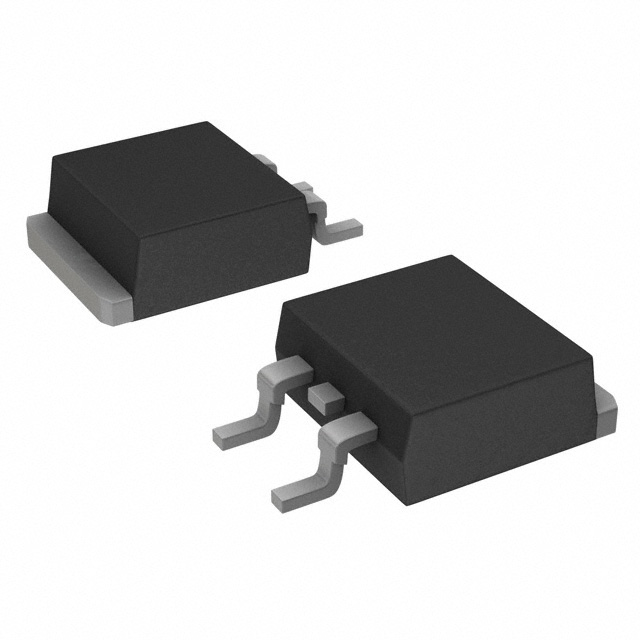
Vishay General Semiconductor - Diodes Division VS-6CWQ06FNTRLPBF
Part No.:
VS-6CWQ06FNTRLPBF
Manufacturer:
Vishay General Semiconductor - Diodes Division
Category:
Diode Arrays
Package:
TO-252-3, DPAK (2 Leads + Tab), SC-63
Datasheet:
AetrixVS-6CWQ06FNTRLPBF.pdf
Description:
DIODE ARRAY SCHOTT 60V 3.5A DPAK
Quantity:
Payment:
Payment
Shipping:
Shipping

Inventory:7,103

Please send an inquiry. Send us your inquiry, and we will respond immediately.

Part Number
Quantity*
Price
Name*
Company
Email*
Comments

Product details

Overview

VS-6CWQ06FNTRLPBF from Vishay Semiconductors is a surface-mount, center-tap dual Schottky rectifier in D-PAK (TO-252AA) package, rated 60 V reverse voltage and 3.5 A average forward current per leg (7 A total device), with low 0.61 V forward voltage at 3 A and 25 °C, used for high-frequency freewheeling and reverse battery protection in DC/DC converters and switching power supplies.

For engineers reviewing the VS-6CWQ06FNTRLPBF datasheet, VS-6CWQ06FNTRLPBF pinout, VS-6CWQ06FNTRLPBF application, or VS-6CWQ06FNTRLPBF equivalent, key selection criteria include its common-cathode dual-leg configuration, 4.70 °C/W junction-to-case thermal resistance per leg, 6 mJ non-repetitive avalanche energy rating, and RoHS-compliant, MSL Level 1 reflow capability.

Technical Context

This dual Schottky rectifier integrates two identical anode terminals sharing a single cathode terminal in a monolithic die structure, enabling synchronous half-wave rectification in center-tapped topologies. Its guard ring design enhances ruggedness against transient overvoltage and thermal stress, supporting reliable operation up to 150 °C junction temperature.

The device operates with low forward voltage drop across its wide temperature range (–40 °C to 150 °C), and exhibits fast recovery characteristics due to absence of minority-carrier storage-confirmed by 10,000 V/μs maximum dV/dt rating and 145 pF typical junction capacitance per leg at 5 V reverse bias.

Key Specifications

ParameterValue and Actual Design Meaning
VR (Max DC Reverse Voltage)60 V - supports input rails up to 48 V nominal systems with margin for transients
IF(AV) per leg3.5 A - enables continuous conduction mode operation in compact 12–24 V DC/DC converters
VF at 3 A, 25 °C0.61 V - reduces forward conduction loss to ~1.83 W per leg, easing thermal management
RthJC per leg4.70 °C/W - allows direct PCB copper pour heatsinking without external heatsink for ≤2.5 W dissipation
EAS per leg6 mJ - withstands inductive turn-off energy in flyback and buck-boost freewheeling paths
CT per leg @ 5 V145 pF - minimizes capacitive loading on high-side switch nodes in synchronous rectifier designs
IRM @ 125 °C30 mA - ensures stable blocking under elevated ambient conditions in enclosed power modules

Pinout & Package

D-PAK (TO-252AA) surface-mount package with exposed thermal pad on underside; 4-pin outline (pins 1–4), lead-free (PbF) finish, MSL Level 1 compliant, 0.3 g mass.

Pin/TerminalCircuit RoleDesign Meaning
Pin 1Anode 1Input terminal for first Schottky diode leg; connects to primary winding tap or switching node
Pin 2Cathode (common)Shared output node for both legs; requires low-inductance PCB trace to ground or output rail
Pin 3Anode 2Input terminal for second Schottky diode leg; used for complementary phase or dual-output rectification
Pin 4Thermal Pad (exposed)Electrically connected to cathode; must be soldered to large copper area for thermal conduction and EMI control

Key Features

FeatureDesign Value
Center-tap common-cathode configurationEnables dual-leg synchronous rectification from single output node-reduces PCB routing complexity vs. discrete diodes
Guard ring constructionImproves edge termination robustness, raising surge immunity and long-term reliability under repetitive dv/dt stress
Low VF slope resistance (34.31 mΩ)Ensures predictable voltage drop increase under dynamic load steps-critical for accurate output voltage regulation
MSL Level 1 reflow ratingPermits standard Pb-free reflow profiles (peak 260 °C) without moisture sensitivity concerns or baking requirements
RoHS-compliant and halogen-freeMeets global environmental compliance mandates for industrial, telecom, and consumer end equipment

Applications

Switching Power Supply Output RectificationBattery Charging Circuit Protection

Use Scenario: Used as secondary-side rectifier in 24 V input, 5–12 V output isolated DC/DC converters with center-tapped transformer.

IC Role / Device Role / Timing Role: Dual-leg Schottky rectifier providing low-loss, high-efficiency synchronous rectification with shared cathode return path.

Use Value: Reduces conduction loss by >35% versus standard PN diodes, lowering thermal footprint and improving full-load efficiency to >92%.

Use Scenario: Placed between Li-ion battery pack and charging controller to prevent reverse current flow during fault or standby.

IC Role / Device Role / Timing Role: Reverse-battery protection diode leveraging low forward voltage and high surge tolerance.

Use Value: Blocks reverse current up to 60 V while maintaining <0.65 V drop at 6 A charge current-minimizing heat generation in space-constrained portable designs.

Flyback Converter Freewheeling DiodeAutomotive Infotainment Power Rail Clamping

Use Scenario: Freewheeling path in 12 V automotive flyback supply powering display backlight and USB ports.

IC Role / Device Role / Timing Role: Fast-recovery freewheeling diode handling discontinuous conduction mode (DCM) transitions.

Use Value: Eliminates reverse recovery tail, reducing EMI and enabling higher switching frequencies (≥300 kHz) without snubber circuits.

Use Scenario: Clamp diode on 5 V USB power rail in head unit to suppress load-dump transients and protect downstream USB controllers.

IC Role / Device Role / Timing Role: Transient voltage suppression via low-VF forward conduction during overvoltage events.

Use Value: Absorbs up to 6 mJ avalanche energy per leg without failure-survives ISO 7637-2 Pulse 5a load-dump spikes without external TVS.

Equivalent & Alternatives

The following parts are listed as comparable options for similar Schottky rectifier applications.

Alternative PartTechnical DifferenceApplication DifferenceSelection Advice
STPS640CWSame D-PAK package, 60 V, 3 A per leg (6 A total); VF = 0.65 V @ 3 A, 25 °C; RthJC = 5.5 °C/W per legLower current rating limits use in >5 A continuous output designs; higher thermal resistance requires larger copper areaSelect when cost sensitivity outweighs marginal efficiency gain and board space permits additional thermal relief
MBR1060CTTO-220AB package, 60 V, 5 A per leg (10 A total); VF = 0.75 V @ 5 A, 25 °C; no MSL ratingThrough-hole mounting incompatible with automated SMT lines; lacks RoHS-compliant reflow profile supportChoose only for legacy through-hole designs or prototyping where thermal mass mitigates peak dissipation

Compared with STPS640CW and MBR1060CT, the VS-6CWQ06FNTRLPBF delivers superior thermal performance (4.70 vs. 5.5 °C/W), tighter VF matching across legs, and full SMT manufacturability-making it optimal for high-density, high-efficiency 3–7 A DC/DC modules targeting automotive and industrial markets.

Availability

VS-6CWQ06FNTRLPBF is available at Aetrix Electronics and suitable for switching power supplies, battery charging systems, and automotive infotainment power rails requiring stable component supply, consistent parametric performance, and long-term production continuity.

Supply support for VS-6CWQ06FNTRLPBF includes scheduled delivery planning, volume procurement assistance, BOM continuity management, traceable sourcing, and lifecycle availability coordination for OEM customers, industrial embedded developers, connected-device designers, and electronics production programs.

Manufacturer

Vishay Semiconductors is a global leader in discrete semiconductors, specializing in high-reliability diodes, MOSFETs, optoelectronics, and passive components for demanding industrial, automotive, and computing applications.

The VS-6CWQ06FNTRLPBF belongs to Vishay's "Q" series of Schottky rectifiers-engineered specifically for high-frequency, high-efficiency power conversion where low forward voltage, fast switching, and rugged thermal performance are critical.

FAQ

What is the maximum average forward current rating per leg for VS-6CWQ06FNTRLPBF?

The VS-6CWQ06FNTRLPBF is rated for 3.5 A average forward current per leg at TC = 133 °C with 50 % duty cycle rectangular waveform. This corresponds to 7 A total device current. Derating is required above 133 °C case temperature, as shown in Figure 5 of the datasheet. The VS-6CWQ06FNTRLPBF maintains this rating under MSL Level 1 reflow conditions and supports sustained operation up to 150 °C junction temperature.

Does VS-6CWQ06FNTRLPBF support lead-free reflow assembly?

Yes, the VS-6CWQ06FNTRLPBF is RoHS-compliant and qualified for lead-free reflow with a maximum peak temperature of 260 °C, meeting MSL Level 1 per J-STD-020. Its PbF marking confirms lead-free terminations and compatibility with standard industry reflow profiles. No pre-baking is required prior to assembly, and the VS-6CWQ06FNTRLPBF retains full electrical specifications after reflow.

What is the pin configuration and thermal pad connection for VS-6CWQ06FNTRLPBF?

The VS-6CWQ06FNTRLPBF uses a 4-pin D-PAK (TO-252AA) outline: Pin 1 = Anode 1, Pin 2 = Common Cathode, Pin 3 = Anode 2, Pin 4 = Exposed Thermal Pad. The thermal pad is electrically tied to the cathode (Pin 2) and must be soldered to a large PCB copper area for thermal conduction and EMI control. The VS-6CWQ06FNTRLPBF datasheet specifies minimum pad dimensions and solder stencil guidelines in Document 95016.

How does the guard ring feature improve reliability of VS-6CWQ06FNTRLPBF?

The guard ring in the VS-6CWQ06FNTRLPBF enhances edge termination robustness, suppressing surface leakage and preventing premature breakdown under high dv/dt or transient overvoltage conditions. This design improves long-term reliability in harsh environments such as automotive load-dump events or industrial motor drive freewheeling paths. The VS-6CWQ06FNTRLPBF demonstrates stable IRM and EAS performance across its full temperature range thanks to this structural reinforcement.

Can VS-6CWQ06FNTRLPBF replace discrete Schottky diodes in center-tapped transformer designs?

Yes, the VS-6CWQ06FNTRLPBF is specifically designed as a drop-in replacement for two discrete Schottky diodes in center-tapped configurations-its common-cathode topology eliminates separate cathode routing and reduces parasitic inductance. Unlike discrete solutions, the VS-6CWQ06FNTRLPBF ensures matched VF and thermal coupling between legs, improving current sharing and system efficiency. It is widely deployed in telecom and server power supplies for this purpose.

VS-6CWQ06FNTRLPBF Specifications

Product attributes
Attribute value
Manufacturer:
Vishay General Semiconductor - Diodes Division
Series:
-
Package/Case:
TO-252-3, DPAK (2 Leads + Tab), SC-63
Packaging:
Tape & Reel (TR)
Product Status:
Obsolete
Diode Configuration:
1 Pair Common Cathode
Technology:
Schottky
Voltage - DC Reverse (Vr) (Max):
60 V
Current - Average Rectified (Io) (per Diode):
3.5A
Voltage - Forward (Vf) (Max) @ If:
610 mV @ 3 A
Speed:
Fast Recovery =< 500ns, > 200mA (Io)
Reverse Recovery Time (trr):
-
Current - Reverse Leakage @ Vr:
2 mA @ 60 V
Operating Temperature - Junction:
-40°C ~ 150°C
Grade:
-
Qualification:
-
Mounting Type:
Surface Mount
Supplier Device Package:
TO-252AA (DPAK)

VS-6CWQ06FNTRLPBF FAQ

1.How can I place an order for VS-6CWQ06FNTRLPBF through Aetrix?

Please submit a Request for Quotation (RFQ) for VS-6CWQ06FNTRLPBF on Aetrix. Our sales agent will provide a competitive quotation and guide you through the order confirmation once you accept the terms.

2.Are the price and stock information for VS-6CWQ06FNTRLPBF reliable?

The price and inventory of VS-6CWQ06FNTRLPBF are updated periodically and may fluctuate due to market conditions. Stock and pricing data are typically refreshed every 24 hours. Quotation validity for VS-6CWQ06FNTRLPBF is usually 5 days.

3.What payment methods are accepted for VS-6CWQ06FNTRLPBF?

We accept Wire Transfer, PayPal, Credit Card, Western Union, MoneyGram, and Escrow for VS-6CWQ06FNTRLPBF transactions.

Note: Certain payment methods may incur a processing fee.

4.How is shipping managed for VS-6CWQ06FNTRLPBF?

VS-6CWQ06FNTRLPBF orders can be shipped via leading logistics carriers, including DHL, UPS, FedEx, TNT, or Registered Mail.

Once your VS-6CWQ06FNTRLPBF order is processed, you will receive an email with the shipment details and tracking number.

Note: Tracking information may take up to 24 hours to appear. Express delivery typically takes 3–5 business days.

5.How can I obtain technical support or documentation for VS-6CWQ06FNTRLPBF?

For technical support, including VS-6CWQ06FNTRLPBF datasheets, pinout diagrams, or application guidance, please contact our engineering support team. They can provide detailed documentation and assistance for your VS-6CWQ06FNTRLPBF requirements.

6.How does Aetrix verify that VS-6CWQ06FNTRLPBF is sourced from the original manufacturer or authorized distributors?

All VS-6CWQ06FNTRLPBF products on Aetrix are procured from qualified distributors and authorized channels. Our dedicated quality assurance team conducts strict verification, including traceability checks and, if necessary, third-party testing. This ensures that VS-6CWQ06FNTRLPBF meets industry standards.

7.What is the process for return or replacement of VS-6CWQ06FNTRLPBF?

All VS-6CWQ06FNTRLPBF units undergo pre-shipment inspection (PSI). If there is an issue with VS-6CWQ06FNTRLPBF, returns or replacements are accepted under the following conditions:

1.Quantity discrepancies, incorrect items, or visible external defects (such as breakage or corrosion), acknowledged by Aetrix.

2.The issue is reported within 90 days of delivery.

3.The VS-6CWQ06FNTRLPBF part is unused and in its original packaging.

Return procedure for VS-6CWQ06FNTRLPBF:

1.Submit a request within 90 days.

2.Obtain a Return Material Authorization (RMA) from Aetrix.

VS-6CWQ06FNTRLPBF Tags
  • VS-6CWQ06FNTRLPBF
  • VS-6CWQ06FNTRLPBF PDF
  • VS-6CWQ06FNTRLPBF Datasheet
  • VS-6CWQ06FNTRLPBF Specifications
  • VS-6CWQ06FNTRLPBF Images
  • Vishay General Semiconductor - Diodes Division
  • Vishay General Semiconductor - Diodes Division VS-6CWQ06FNTRLPBF
  • Buy VS-6CWQ06FNTRLPBF
  • VS-6CWQ06FNTRLPBF Price
  • VS-6CWQ06FNTRLPBF Distributor
  • VS-6CWQ06FNTRLPBF Supplier
  • VS-6CWQ06FNTRLPBF Wholesale
Related Products
BAV99-7-F
BAV99-7-F

Diodes Incorporated

BAT54C-7-F
BAT54C-7-F

Diodes Incorporated

BAV99,215
BAV99,215

Nexperia USA Inc.

BAT54SLT1G
BAT54SLT1G

onsemi

BAV70LT1G
BAV70LT1G

onsemi

BAT54CLT1G
BAT54CLT1G

onsemi

BAT54S-7-F
BAT54S-7-F

Diodes Incorporated

BAV99LT1G
BAV99LT1G

onsemi

BAT54S,215
BAT54S,215

Nexperia USA Inc.

BAS40-04LT1G
BAS40-04LT1G

onsemi

MMBD1503-TP
MMBD1503-TP

Micro Commercial Co

BAV99WT1G
BAV99WT1G

onsemi

Tech Hub

Search

Search

PRODUCT

PRODUCT

PHONE

PHONE

USER

USER