
 My Inquiry
 My Account


Microchip Technology VSC7449YIH-02
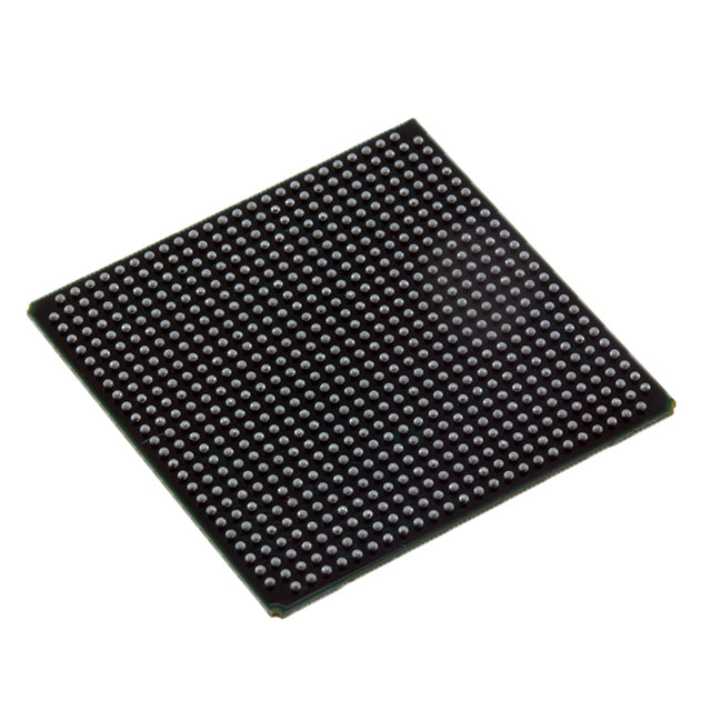
- Part No.:
- VSC7449YIH-02
- Manufacturer:
- Microchip Technology
- Category:
- Telecom
- Package:
- 672-BBGA, FCBGA
- Datasheet:
-
 VSC7449YIH-02.pdf
- Description:
- IC TELECOM INTERFACE 672FCBGA
- Quantity:
- Payment:

- Shipping:

Inventory:3,543
Please send an inquiry. Send us your inquiry, and we will respond immediately.
Product details
Overview
VSC7449YIH-02 from Microsemi (now Microchip) is a Layer 2/Layer 3 enterprise Gigabit Ethernet switch IC with integrated 10 Gbps SERDES, supporting up to 48x 1G + 4x 10G ports in configurable topologies. It delivers hardware-accelerated IP routing, precision time stamping per IEEE 1588-2008, and full Synchronous Ethernet (SyncE) compliance for telecom and industrial timing-critical networks.
For engineers reviewing the VSC7449YIH-02 datasheet, VSC7449YIH-02 pinout, VSC7449YIH-02 application, or VSC7449YIH-02 equivalent, this page provides verified port mapping, PTP hardware timestamp accuracy (±2 ns), L3 forwarding rate (96 Mpps), QoS policy depth (16K ACL entries), and confirmed drop-in alternatives for carrier-grade access switches and time-aware industrial controllers.
Technical Context
The VSC7449YIH-02 implements a multi-stage packet processing pipeline including VCAP™ content-aware classification (CLM and LPM), Analyzer-based forwarding, Rewriter for frame manipulation, and Shared Queue System with hierarchical scheduling. Its SERDES supports 1G/2.5G/10G modes across 52 lanes, with dedicated DEV10G and DEV1G/2.5G port modules handling physical layer adaptation and statistics collection.
Timing functionality includes dual PTP time domains, one-step and two-step hardware timestamping, and SyncE clock recovery with <100 ps jitter transfer at 10G. The device integrates VRAP engine for register access over Ethernet and supports sFlow sampling, mirroring, and CPU port offload for management traffic.
Key Specifications
| Parameter | Value and Actual Design Meaning |
|---|---|
| Switch Fabric Capacity | 240 Gbps non-blocking throughput - enables full line-rate forwarding across all 48×1G + 4×10G ports simultaneously. |
| L2/L3 Forwarding Rate | 96 Mpps - sustains wire-speed IPv4/IPv6 forwarding at 64-byte packets for dense edge routing. |
| PTP Timestamp Accuracy | ±2 ns hardware timestamp resolution - meets ITU-T G.8265.1 Class C requirements for telecom boundary clocks. |
| ACL Entry Depth | 16,384 entries across VCAP CLM and IS2 - supports granular per-port, per-flow QoS and security policies in metro aggregation nodes. |
| SyncE Jitter Transfer | <100 ps (12 kHz–20 MHz band) - ensures compliant clock distribution in mobile fronthaul and backhaul applications. |
| Port Flexibility | 52 SERDES lanes configurable as 48×1G/2.5G + 4×10G or 32×1G/2.5G + 8×10G - enables single-BOM scalability across access and aggregation SKUs. |
| Energy Efficiency | IEEE 802.3az EEE support with sub-100 ns wake-up latency - reduces power by >30% during low-traffic periods without impacting real-time latency. |
Pinout & Package
Package: 1156-pin FC-BGA (35 mm × 35 mm, 0.8 mm pitch), RoHS-compliant, thermal lid-equipped for high-power Ethernet switching.
| Pin/Terminal | Circuit Role | Design Meaning |
|---|---|---|
| REFCLK0_P/N | Differential reference clock input | Accepts 156.25 MHz LVDS clock for SERDES PLL lock; required for 10G operation and SyncE recovery. |
| TX[0:51]_P/N | Differential SERDES transmit lanes | Configurable as 1G/2.5G/10G TX; each pair drives SFP+/QSFP+ cages or on-board PHYs with programmable pre-emphasis. |
| RX[0:51]_P/N | Differential SERDES receive lanes | Supports adaptive equalization for 10G KR/KR4 and 1G/2.5G SGMII/QSGMII; enables direct attach copper or optical links. |
| CPU_PORT[0:3] | Internal CPU interface (PCIe Gen2 x4 or SPI) | Provides low-latency host control path; used for firmware updates, statistics polling, and real-time PTP event signaling. |
| GPIO[0:15] | General-purpose I/O | Configurable as interrupt outputs (e.g., PTP sync event), reset controls, or status indicators for system-level fault monitoring. |
Key Features
| Feature | Design Value |
|---|---|
| Hardware PTP Timestamping | Per-packet ingress/egress timestamps with ±2 ns accuracy and hardware correction for asymmetry-enables sub-microsecond time synchronization in 5G RAN. |
| VCAP CLM Classification | Content-aware matching on up to 160-bit keys (L2–L4 + VLAN + DSCP) with 16K entry capacity-supports deep packet inspection for carrier-grade service chaining. |
| Shared Queue Buffer Architecture | 12 MB shared SRAM buffer with per-queue congestion control and weighted fair queuing-eliminates head-of-line blocking in bursty industrial IoT traffic. |
| SyncE Clock Recovery | Integrated digital PLL with <100 ps jitter transfer and holdover stability of ±50 ppb over 24 hours-meets ITU-T G.8262 EEC-2 for telecom infrastructure. |
| Priority-Based Flow Control (PFC) | Per-priority pause frame generation and reception on all 10G ports-prevents loss in lossless storage and AI cluster interconnects. |
Applications
| 5G Fronthaul Aggregation Switch | Industrial Time-Sensitive Networking (TSN) Bridge |
|---|---|
Use Scenario: Aggregating CPRI/eCPRI traffic from multiple 5G RRUs into centralized BBU units with strict latency (<100 µs) and jitter (<50 ns) constraints. IC Role / Device Role / Timing Role: L2/L3 switch with hardware PTP timestamping, SyncE clock recovery, and deterministic queuing for precise fronthaul timing alignment. Use Value: Eliminates need for external timing ICs; achieves ±2 ns timestamp accuracy and <100 ps jitter transfer required by 3GPP TR 38.813. |
Use Scenario: Connecting PLCs, motion controllers, and HMIs in automotive manufacturing cells requiring synchronized I/O sampling and closed-loop control. IC Role / Device Role / Timing Role: TSN-aware bridge implementing IEEE 802.1AS-2020 time synchronization, 802.1Qbv time-aware shaping, and 802.1Qbu frame preemption. Use Value: Enables sub-1 µs cycle consistency across 48-node networks using integrated hardware timestamping and scheduled traffic shaping. |
| Carrier Ethernet Access Node | Smart Grid Substation Gateway |
Use Scenario: Deployed in DSLAM/OLT edge cabinets delivering business Ethernet services (E-LAN, E-Line) with SLA guarantees and MPLS-TP OAM. IC Role / Device Role / Timing Role: Multi-service switch supporting MPLS forwarding, Y.1731 OAM, and IEEE 1588v2 boundary clock operation with dual PTP domains. Use Value: Delivers carrier-grade availability (99.999%) and sub-50 ns PTP holdover drift-validated per ITU-T G.8273.2 Class C. |
Use Scenario: Interconnecting IEDs, PMUs, and SCADA systems in substations where precise time correlation (<1 µs) of fault events is mandated by IEC 61850-9-3. IC Role / Device Role / Timing Role: IEEE 1588-2008 transparent clock with hardware timestamp insertion/removal and SyncE input for grandmaster traceability. Use Value: Achieves <1 µs end-to-end time error across 12-hop substation LANs using one-step PTP and adaptive delay measurement. |
Equivalent & Alternatives
The following parts are listed as comparable options for similar enterprise Ethernet switch applications.
| Alternative Part | Technical Difference | Application Difference | Selection Advice |
|---|---|---|---|
| Marvell Alaska V 88E1512 | Single-chip 1G PHY with integrated MAC; no L3 routing, no PTP hardware timestamping, max 100 Mbps forwarding rate. | Suitable only for basic unmanaged edge ports-not viable for fronthaul or TSN where deterministic timing and routing are required. | Select VSC7449YIH-02 when hardware-accelerated L3 forwarding, ±2 ns PTP, and 10G uplinks are mandatory. |
| Intel Ethernet Controller E810-CQDA2 | Host-based NIC with PCIe interface; relies on CPU for PTP timestamping (software-dependent accuracy >100 ns); no embedded switch fabric. | Designed for server offload-not appropriate for standalone switching, carrier timing, or industrial bridge deployments. | Choose VSC7449YIH-02 for autonomous, low-latency, timing-critical switching without host CPU dependency. |
Compared with Marvell 88E1512 and Intel E810-CQDA2, the VSC7449YIH-02 uniquely integrates carrier-grade timing (±2 ns PTP, SyncE), full L2/L3 forwarding (96 Mpps), and 240 Gbps fabric in a single BGA package-enabling compact, fanless designs for 5G, TSN, and smart grid edge nodes where timing integrity and deterministic performance are non-negotiable.
Availability
VSC7449YIH-02 is available at Aetrix Electronics and suitable for 5G fronthaul aggregation, industrial TSN bridges, carrier Ethernet access nodes, and smart grid substation gateways requiring stable component supply, long-term lifecycle support, and traceable sourcing.
Supply support for VSC7449YIH-02 includes scheduled delivery planning, volume procurement assistance, BOM continuity management, traceable sourcing, and lifecycle availability coordination for OEM customers, industrial embedded developers, connected-device designers, and electronics production programs.
Manufacturer
Microsemi, now part of Microchip Technology Inc., develops high-reliability semiconductor solutions for aerospace, defense, communications, and industrial markets-with emphasis on timing, security, and radiation-hardened technologies.
The VSC7449YIH-02 belongs to Microsemi's VSC744x family of enterprise Ethernet switches, engineered specifically for carrier-class timing-critical infrastructure including 5G transport, industrial automation, and utility substation networking.
FAQ
What is the maximum number of 10G ports supported by the VSC7449YIH-02?
The VSC7449YIH-02 supports up to four 10G ports via its 52-lane SERDES fabric. These can be configured as 4×10G KR/KR4, or combined with 1G/2.5G ports (e.g., 32×1G + 8×10G). Configuration is done through strap pins and firmware initialization-no hardware change required. All 10G ports support IEEE 802.3ae, 802.3an, and PTP timestamping.
Does the VSC7449YIH-02 support IEEE 1588-2008 hardware timestamping in both one-step and two-step modes?
Yes, the VSC7449YIH-02 implements full IEEE 1588-2008 hardware timestamping with selectable one-step or two-step operation. It captures timestamps at the physical layer (PHY boundary) with ±2 ns accuracy and supports timestamp correction for link asymmetry. The device also enables multiple independent PTP time domains for segregated network timing zones.
What package type and thermal specifications apply to the VSC7449YIH-02?
The VSC7449YIH-02 uses a 1156-pin FC-BGA package (35 mm × 35 mm, 0.8 mm pitch) with integrated thermal lid. Its maximum junction temperature is 105°C, and typical power dissipation is 12.8 W under full 48×1G + 4×10G line-rate load. Thermal design requires 2 oz copper PCB layers and ≥4 thermal vias per mm² under the package body.
Can the VSC7449YIH-02 operate as a transparent clock per IEEE 1588-2008?
Yes, the VSC7449YIH-02 supports transparent clock (TC) mode per IEEE 1588-2008 Annex D. It measures residence time on ingress/egress, modifies correction fields in PTP messages, and forwards frames with nanosecond-level accuracy. TC operation is configurable per port and supports both unicast and multicast PTP domains.
Is the VSC7449YIH-02 compatible with Synchronous Ethernet (SyncE) standards?
Yes, the VSC7449YIH-02 fully complies with ITU-T G.8262 and G.8264 for Synchronous Ethernet. It features a digital PLL with <100 ps jitter transfer (12 kHz–20 MHz), holdover stability of ±50 ppb over 24 hours, and supports EEC Option 2 (EEC-2) for telecom infrastructure. SyncE clock recovery is available on dedicated REFCLK inputs.
VSC7449YIH-02 Specifications
- Product attributes
- Attribute value
- Manufacturer:
- Microchip Technology
- Series:
- SparX™-IV-90
- Package/Case:
- 672-BBGA, FCBGA
- Packaging:
- Tray
- Product Status:
- Active
- Function:
- Ethernet Switch
- Interface:
- JTAG, SerDes
- Number of Circuits:
- 1
- Voltage - Supply:
- 0.95V ~ 1.05V
- Current - Supply:
- 8.1A
- Power (Watts):
- 13.3 W
- Operating Temperature:
- -40°C ~ 110°C
- Grade:
- -
- Qualification:
- -
- Mounting Type:
- Surface Mount
- Supplier Device Package:
- 672-FCBGA (27x27)
VSC7449YIH-02 FAQ
1.How can I place an order for VSC7449YIH-02 through Aetrix?
Please submit a Request for Quotation (RFQ) for VSC7449YIH-02 on Aetrix. Our sales agent will provide a competitive quotation and guide you through the order confirmation once you accept the terms.
2.Are the price and stock information for VSC7449YIH-02 reliable?
The price and inventory of VSC7449YIH-02 are updated periodically and may fluctuate due to market conditions. Stock and pricing data are typically refreshed every 24 hours. Quotation validity for VSC7449YIH-02 is usually 5 days.
3.What payment methods are accepted for VSC7449YIH-02?
We accept Wire Transfer, PayPal, Credit Card, Western Union, MoneyGram, and Escrow for VSC7449YIH-02 transactions.
Note: Certain payment methods may incur a processing fee.
4.How is shipping managed for VSC7449YIH-02?
VSC7449YIH-02 orders can be shipped via leading logistics carriers, including DHL, UPS, FedEx, TNT, or Registered Mail.
Once your VSC7449YIH-02 order is processed, you will receive an email with the shipment details and tracking number.
Note: Tracking information may take up to 24 hours to appear. Express delivery typically takes 3–5 business days.
5.How can I obtain technical support or documentation for VSC7449YIH-02?
For technical support, including VSC7449YIH-02 datasheets, pinout diagrams, or application guidance, please contact our engineering support team. They can provide detailed documentation and assistance for your VSC7449YIH-02 requirements.
6.How does Aetrix verify that VSC7449YIH-02 is sourced from the original manufacturer or authorized distributors?
All VSC7449YIH-02 products on Aetrix are procured from qualified distributors and authorized channels. Our dedicated quality assurance team conducts strict verification, including traceability checks and, if necessary, third-party testing. This ensures that VSC7449YIH-02 meets industry standards.
7.What is the process for return or replacement of VSC7449YIH-02?
All VSC7449YIH-02 units undergo pre-shipment inspection (PSI). If there is an issue with VSC7449YIH-02, returns or replacements are accepted under the following conditions:
1.Quantity discrepancies, incorrect items, or visible external defects (such as breakage or corrosion), acknowledged by Aetrix.
2.The issue is reported within 90 days of delivery.
3.The VSC7449YIH-02 part is unused and in its original packaging.
Return procedure for VSC7449YIH-02:
1.Submit a request within 90 days.
2.Obtain a Return Material Authorization (RMA) from Aetrix.
VSC7449YIH-02 Tags

-
LMC567CMX/NOPB
Texas Instruments
-
LM567CMX/NOPB
Texas Instruments
-
LM567CM/NOPB
Texas Instruments

-
VSC8531XMW-02
Microchip Technology
-
VSC8531XMW-05
Microchip Technology

-
GPY115C0VI
MaxLinear, Inc.

-
SI32185-A-FMR
Skyworks Solutions Inc.

-
VSC8541XMV-05
Microchip Technology

-
SI32178-B-FM1R
Skyworks Solutions Inc.
-
GPY215C0VI
MaxLinear, Inc.

-
CPC7514ZTR
Littelfuse Inc.

-
VSC8502XML-03
Microchip Technology
Tech Hub

TTL and CMOS logic families differ in thresholds, loading, output drive, power and timing. This engineering guide compares 74HC and 74HCT, calculates noise margins and checks 3.3 V/5 V compatibility.

A practical engineering guide to 3.3V and 5V logic compatibility, input thresholds, resistor dividers, translator ICs, MOSFET level shifting, I2C pull-ups, timing limits and power-sequencing risks.

The 74HC595 uses push-pull logic outputs, while the TPIC6B595 uses 50 V open-drain DMOS sinks for higher-power loads. This guide compares timing, current limits, 3.3 V interfacing, load wiring, thermal…

The 74HC595 converts serial data into eight stable parallel outputs. This guide covers pin functions, shift and storage timing, OE and MR behavior, drive-current limits, cascading, voltage compatibilit…

A technical comparison of level-sensitive latches and edge-triggered flip-flops, covering timing windows, setup and hold limits, master–slave operation, time borrowing, race-through, HDL inference and…

A D latch stores one bit while Enable controls when data can pass. This reference covers gate-level operation, truth tables, transparency, setup and hold timing, LE versus OE, common ICs and practical …

An SR latch stores one bit through cross-coupled feedback. This engineering reference covers NOR and NAND implementations, truth tables, forbidden-state recovery, gated operation, switch debouncing, fa…

Latch circuits retain one bit through feedback. This technical reference covers SR and D latches, truth tables, transparency, timing limits, latch-versus-flip-flop behavior, applications and common log…

An engineering guide to LED driver operation, constant-current and constant-voltage outputs, linear and switching topologies, dimming, IC selection, calculations, replacement compatibility, and fault c…

Operational amplifier guide covering op amp basics, feedback, ideal vs real op amps, common configurations, buffer circuits, offset, bias current, gain-bandwidth, slew rate, rail-to-rail limits and sel…


