
 My Inquiry
 My Account


Microchip Technology VSC8486YSN-04
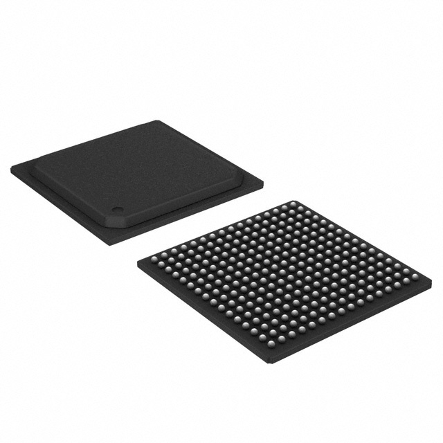
- Part No.:
- VSC8486YSN-04
- Manufacturer:
- Microchip Technology
- Category:
- Telecom
- Package:
- 256-BBGA, FCBGA
- Datasheet:
-
 VSC8486YSN-04.pdf
- Description:
- IC TELECOM INTERFACE 256FCBGA
- Quantity:
- Payment:

- Shipping:

Inventory:2,021
Please send an inquiry. Send us your inquiry, and we will respond immediately.
Product details
Overview
VSC8486YSN-04 from Microsemi (now Microchip) is a 10 Gbps LAN/WAN transceiver supporting XAUI or XGMII to XFI conversion, compliant with IEEE 802.3ae, ITU-T G.709, and SONET/SDH standards. It integrates PMA, PCS, WIS, and PHY-XS layers in a single die, operates at 3.3 V and 1.2 V supplies, and supports WAN mode with FEC for optical transport applications.
For engineers reviewing the VSC8486YSN-04 datasheet, VSC8486YSN-04 pinout, VSC8486YSN-04 application, or VSC8486YSN-04 equivalent, key selection criteria include XFI CML output compliance, XAUI/XGMII interface flexibility, synchronous Ethernet support, WAN framing capability, and integrated loopback modes for system validation.
Technical Context
The VSC8486YSN-04 implements a full 10-Gigabit Ethernet physical layer stack: XAUI receiver with lane deskew and 10b/8b decoding, XGMII extender, 64b/66b PCS with FEC controls, WAN Interface Sublayer (WIS) for SONET/SDH mapping, and PMA with CML XFI transmitter (pre-emphasis adjustable) and receiver (equalization enabled). It supports both LAN (IEEE 802.3ae) and WAN (G.709) modes via register configuration.
Its dual-reference-clock architecture enables synchronous Ethernet operation in conventional and enhanced modes, with programmable phase detector outputs and external PLL support. Loopback paths span PHY-XS (shallow/deep), PCS FIFO, PMA, and split-lane configurations - enabling comprehensive signal integrity and protocol-layer testing without external equipment.
Key Specifications
| Parameter | Value and Actual Design Meaning |
|---|---|
| Data Rate | 10.3125 Gbps line rate for XFI; supports 10GBASE-R and OTU-2 (10.709 Gbps) WAN mode. |
| Interface Standards | Complies with IEEE 802.3ae (XAUI/XGMII-to-XFI), ITU-T G.709 (OTN), and SONET OC-192/SDH STM-64. |
| Power Supply | 3.3 V for I/O and analog blocks; 1.2 V core supply; typical total power consumption ≤ 2.1 W. |
| XFI Output | CML differential output with programmable pre-emphasis (0–12 dB) and slew rate control for fiber module interfacing. |
| Loopback Modes | 11 distinct internal loopbacks including PHY-XS deep/shallow, PCS FIFO, PMA, and XAUI/PMA split configurations. |
| Synchronous Ethernet | Supports SyncE in conventional (recovered clock forwarding) and enhanced (phase-aligned ESMC-aware) modes per ITU-T G.8262. |
| Operating Temp | Industrial grade: –40°C to +85°C ambient temperature range, qualified per JEDEC JESD22-A104. |
Pinout & Package
The VSC8486YSN-04 is housed in a 256-pin, 17 mm × 17 mm, 0.8 mm pitch LQFP package with exposed thermal pad. Pin assignments are defined across six functional groups: XFI high-speed serial I/O (differential pairs), XAUI/XGMII parallel interfaces (LVCMOS/LVTTL), reference clocks (LVPECL/LVDS compatible inputs), MDIO/TWI/JTAG management interfaces, status/control signals (LOS, LOM, TX_DISABLE), and multi-rail power/ground distribution.
| Pin/Terminal | Circuit Role | Design Meaning |
|---|---|---|
| XFI_P/N[0:3] | XFI differential transmit/receive lanes | Four CML lanes for 10.3125 Gbps serial data; require AC-coupling and 100 Ω differential termination. |
| XAUI_RX[0:3]_P/N | XAUI differential receive lanes | Four 3.125 Gbps differential inputs with built-in CDR and lane deskew; support AC-coupled backplane traces. |
| XGMII_TXD[0:31] | XGMII transmit data bus | 32-bit LVCMOS interface running at 156.25 MHz; synchronous to TX_CLK, used for MAC-side connection. |
| MDIO / MDC | Management Data Input/Output | IEEE 802.3-compliant two-wire serial interface for register read/write access and device configuration. |
| REFCLK_IN | Reference clock input | Accepts 156.25 MHz (LAN) or 625 MHz (WAN) LVPECL/LVDS; drives internal CMU for clock multiplication. |
| LOS | Loss of Signal indicator | Open-drain active-low output signaling loss of valid XFI input signal; used for system fault monitoring. |
Key Features
| Feature | Design Value |
|---|---|
| Multi-protocol framing | Single-device support for IEEE 802.3ae LAN and ITU-T G.709 WAN modes via software-selectable configuration registers. |
| Integrated FEC engine | Forward Error Correction compliant with G.709 OTU2, reducing bit error rate in long-haul optical links without external logic. |
| Programmable XFI output | Adjustable pre-emphasis (0–12 dB) and slew rate enable optimization for varying PCB trace lengths and SFP+/XFP module characteristics. |
| Comprehensive loopback suite | 11 hardware-accelerated loopback paths spanning PHY-XS, PCS, WIS, and PMA layers - enabling isolated layer-by-layer validation. |
| Synchronous Ethernet support | Dual-mode SyncE implementation (conventional + enhanced) meets G.8262 Class E requirements for phase accuracy and wander tolerance. |
Applications
| 10GbE Line Cards | OTN Transport Terminals |
|---|---|
Use Scenario: High-density 10 Gigabit Ethernet switching line cards in carrier-grade routers requiring low-latency, standards-compliant SerDes interfacing. IC Role / Device Role / Timing Role: Acts as the physical layer bridge between MAC (via XGMII) and optical modules (via XFI), handling encoding, framing, and clock recovery. Use Value: Eliminates need for discrete PCS/WIS/PMA chips; reduces BOM count and board area while ensuring IEEE 802.3ae and G.709 interoperability. | Use Scenario: Optical transport network (OTN) terminals aggregating multiple client services into OTU-2 frames for DWDM transmission. IC Role / Device Role / Timing Role: Performs G.709 OTU-2 framing, FEC insertion, and WAN-mode clock multiplication for SONET/SDH-compatible line rates. Use Value: Enables single-chip OTN framer + SerDes functionality, supporting deterministic latency and BER < 10⁻¹⁵ with integrated FEC. |
| SyncE Timing Equipment | Test & Measurement Platforms |
Use Scenario: Synchronous Ethernet grandmaster clocks and boundary clocks requiring precise phase alignment and ESMC processing. IC Role / Device Role / Timing Role: Provides recovered clock output with sub-nanosecond phase stability and ESMC-aware timing recovery in enhanced SyncE mode. Use Value: Meets ITU-T G.8262 Class E wander and jitter specs without external timing ICs or complex PLL networks. | Use Scenario: Protocol-aware bit-error-rate testers and network analyzers needing flexible, reconfigurable 10G SerDes stimulus and response generation. IC Role / Device Role / Timing Role: Delivers deterministic loopback paths, pattern generator/checker, and statistical counters for layer-specific diagnostics. Use Value: Enables in-system validation of XAUI, XGMII, and XFI signal integrity and protocol conformance without external test fixtures. |
Equivalent & Alternatives
The following parts are listed as comparable options for similar 10G LAN/WAN transceiver applications.
| Alternative Part | Technical Difference | Application Difference | Selection Advice |
|---|---|---|---|
| Marvell Alaska X 88X3310 | Single-lane XFI output only; no WAN framing or WIS layer; supports KR/KX4 but not XAUI. | Limited to LAN-only 10GBASE-R applications; lacks OTN/SONET support and SyncE timing features. | Select when cost-sensitive LAN switch designs require only IEEE 802.3ae compliance and minimal feature set. |
| Intel Ethernet Controller X710-AT2 | MAC+PHY SoC with integrated PCIe host interface; no standalone XAUI/XGMII support; fixed XFI output. | Designed for server NICs, not line-card or transport equipment; no register-level WIS or FEC control. | Choose for embedded server connectivity where host CPU offload and PCIe integration outweigh protocol flexibility. |
Compared with VSC8486YSN-04, the Marvell 88X3310 offers lower power and simpler layout but omits WAN framing and SyncE - making it unsuitable for OTN or telecom timing systems. The Intel X710-AT2 integrates host interface logic but sacrifices configurability and layer-specific diagnostics essential for carrier infrastructure development.
Availability
VSC8486YSN-04 is available at Aetrix Electronics and suitable for 10GbE line cards, OTN transport terminals, SyncE timing equipment, and test & measurement platforms requiring stable component supply, long-term lifecycle assurance, and full documentation traceability.
Supply support for VSC8486YSN-04 includes scheduled delivery planning, volume procurement assistance, BOM continuity management, traceable sourcing, and lifecycle availability coordination for OEM customers, industrial embedded developers, connected-device designers, and electronics production programs.
Manufacturer
Microsemi - now part of Microchip Technology - specializes in high-reliability semiconductor solutions for aerospace, defense, communications, and data center markets, with leadership in timing, RF, and secure communications ICs.
The VSC8486YSN-04 belongs to Microsemi's Precision Timing and Ethernet Transceiver product line, engineered specifically for carrier-class networking equipment requiring multi-standard 10G SerDes, WAN framing, and synchronous Ethernet compliance.
FAQ
What protocols does the VSC8486YSN-04 support natively?
The VSC8486YSN-04 natively supports IEEE 802.3ae (10GBASE-R), ITU-T G.709 (OTU-2), and SONET OC-192/SDH STM-64 protocols through integrated PMA, PCS, WIS, and PHY-XS layers. It performs full 64b/66b encoding, G.709 framing with FEC, and WAN-mode clock multiplication without external logic. All protocol modes are selectable via register configuration in the VSC8486YSN-04.
Does the VSC8486YSN-04 support both XAUI and XGMII host interfaces?
Yes, the VSC8486YSN-04 supports both XAUI (4×3.125 Gbps differential) and XGMII (32-bit LVCMOS at 156.25 MHz) as parallel host-side interfaces. Mode selection is controlled by strap pins and registers; XAUI is typically used for backplane interconnects, while XGMII connects directly to MACs. Both interfaces feed into the same PHY-XS layer before conversion to XFI in the VSC8486YSN-04.
What is the function of the LOS pin on the VSC8486YSN-04?
The LOS (Loss of Signal) pin on the VSC8486YSN-04 is an open-drain, active-low output that asserts when valid XFI input signal amplitude falls below detection threshold for > 100 µs. It interfaces directly with system fault monitors or FPGA GPIOs for link health reporting. LOS behavior is configurable via WIS registers and remains active during all operational modes of the VSC8486YSN-04.
Can the VSC8486YSN-04 operate in synchronous Ethernet enhanced mode?
Yes, the VSC8486YSN-04 supports synchronous Ethernet enhanced mode per ITU-T G.8262, using ESMC (Ethernet Synchronization Messaging Channel) to recover and align phase from incoming traffic. In this mode, it delivers sub-50 ps phase error and meets Class E wander specifications. Enhanced mode requires MDIO configuration of SyncE registers and is fully implemented in hardware within the VSC8486YSN-04.
How many internal loopback modes does the VSC8486YSN-04 provide?
The VSC8486YSN-04 provides 11 distinct internal loopback modes, including PHY-XS shallow/deep, PCS FIFO, PMA, WIS, and split-lane variants (XAUI Split Loopbacks B/D and PMA Split Loopbacks J/K). These are accessible via MDIO register writes and enable isolated testing of each protocol layer without external loopback cables or instruments - a key diagnostic capability of the VSC8486YSN-04.
VSC8486YSN-04 Specifications
- Product attributes
- Attribute value
- Manufacturer:
- Microchip Technology
- Series:
- -
- Package/Case:
- 256-BBGA, FCBGA
- Packaging:
- Tray
- Product Status:
- Active
- Function:
- Transceiver
- Interface:
- Serial
- Number of Circuits:
- 1
- Voltage - Supply:
- 1.2V
- Current - Supply:
- -
- Power (Watts):
- -
- Operating Temperature:
- -
- Grade:
- -
- Qualification:
- -
- Mounting Type:
- Surface Mount
- Supplier Device Package:
- 256-FCBGA (17x17)
VSC8486YSN-04 FAQ
1.How can I place an order for VSC8486YSN-04 through Aetrix?
Please submit a Request for Quotation (RFQ) for VSC8486YSN-04 on Aetrix. Our sales agent will provide a competitive quotation and guide you through the order confirmation once you accept the terms.
2.Are the price and stock information for VSC8486YSN-04 reliable?
The price and inventory of VSC8486YSN-04 are updated periodically and may fluctuate due to market conditions. Stock and pricing data are typically refreshed every 24 hours. Quotation validity for VSC8486YSN-04 is usually 5 days.
3.What payment methods are accepted for VSC8486YSN-04?
We accept Wire Transfer, PayPal, Credit Card, Western Union, MoneyGram, and Escrow for VSC8486YSN-04 transactions.
Note: Certain payment methods may incur a processing fee.
4.How is shipping managed for VSC8486YSN-04?
VSC8486YSN-04 orders can be shipped via leading logistics carriers, including DHL, UPS, FedEx, TNT, or Registered Mail.
Once your VSC8486YSN-04 order is processed, you will receive an email with the shipment details and tracking number.
Note: Tracking information may take up to 24 hours to appear. Express delivery typically takes 3–5 business days.
5.How can I obtain technical support or documentation for VSC8486YSN-04?
For technical support, including VSC8486YSN-04 datasheets, pinout diagrams, or application guidance, please contact our engineering support team. They can provide detailed documentation and assistance for your VSC8486YSN-04 requirements.
6.How does Aetrix verify that VSC8486YSN-04 is sourced from the original manufacturer or authorized distributors?
All VSC8486YSN-04 products on Aetrix are procured from qualified distributors and authorized channels. Our dedicated quality assurance team conducts strict verification, including traceability checks and, if necessary, third-party testing. This ensures that VSC8486YSN-04 meets industry standards.
7.What is the process for return or replacement of VSC8486YSN-04?
All VSC8486YSN-04 units undergo pre-shipment inspection (PSI). If there is an issue with VSC8486YSN-04, returns or replacements are accepted under the following conditions:
1.Quantity discrepancies, incorrect items, or visible external defects (such as breakage or corrosion), acknowledged by Aetrix.
2.The issue is reported within 90 days of delivery.
3.The VSC8486YSN-04 part is unused and in its original packaging.
Return procedure for VSC8486YSN-04:
1.Submit a request within 90 days.
2.Obtain a Return Material Authorization (RMA) from Aetrix.
VSC8486YSN-04 Tags

-
LMC567CMX/NOPB
Texas Instruments
-
LM567CMX/NOPB
Texas Instruments
-
LM567CM/NOPB
Texas Instruments

-
VSC8531XMW-02
Microchip Technology
-
VSC8531XMW-05
Microchip Technology

-
GPY115C0VI
MaxLinear, Inc.

-
SI32185-A-FMR
Skyworks Solutions Inc.

-
VSC8541XMV-05
Microchip Technology

-
SI32178-B-FM1R
Skyworks Solutions Inc.
-
GPY215C0VI
MaxLinear, Inc.

-
CPC7514ZTR
Littelfuse Inc.

-
VSC8502XML-03
Microchip Technology
Tech Hub

TTL and CMOS logic families differ in thresholds, loading, output drive, power and timing. This engineering guide compares 74HC and 74HCT, calculates noise margins and checks 3.3 V/5 V compatibility.

A practical engineering guide to 3.3V and 5V logic compatibility, input thresholds, resistor dividers, translator ICs, MOSFET level shifting, I2C pull-ups, timing limits and power-sequencing risks.

The 74HC595 uses push-pull logic outputs, while the TPIC6B595 uses 50 V open-drain DMOS sinks for higher-power loads. This guide compares timing, current limits, 3.3 V interfacing, load wiring, thermal…

The 74HC595 converts serial data into eight stable parallel outputs. This guide covers pin functions, shift and storage timing, OE and MR behavior, drive-current limits, cascading, voltage compatibilit…

A technical comparison of level-sensitive latches and edge-triggered flip-flops, covering timing windows, setup and hold limits, master–slave operation, time borrowing, race-through, HDL inference and…

A D latch stores one bit while Enable controls when data can pass. This reference covers gate-level operation, truth tables, transparency, setup and hold timing, LE versus OE, common ICs and practical …

An SR latch stores one bit through cross-coupled feedback. This engineering reference covers NOR and NAND implementations, truth tables, forbidden-state recovery, gated operation, switch debouncing, fa…

Latch circuits retain one bit through feedback. This technical reference covers SR and D latches, truth tables, transparency, timing limits, latch-versus-flip-flop behavior, applications and common log…

An engineering guide to LED driver operation, constant-current and constant-voltage outputs, linear and switching topologies, dimming, IC selection, calculations, replacement compatibility, and fault c…

Operational amplifier guide covering op amp basics, feedback, ideal vs real op amps, common configurations, buffer circuits, offset, bias current, gain-bandwidth, slew rate, rail-to-rail limits and sel…


