
 My Inquiry
 My Account


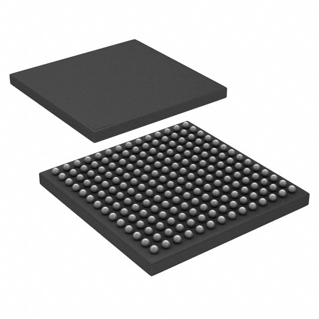
Microchip Technology VSC8489YJU-02
- Part No.:
- VSC8489YJU-02
- Manufacturer:
- Microchip Technology
- Category:
- Telecom
- Package:
- 196-LBGA, FCBGA
- Datasheet:
-
 VSC8489YJU-02.pdf
- Description:
- IC TELECOM INTERFACE 196FCBGA
- Quantity:
- Payment:

- Shipping:

Inventory:291
Please send an inquiry. Send us your inquiry, and we will respond immediately.
Product details
Overview
VSC8489YJU-02 from Microsemi (now Microchip) is a dual-channel 10 GbE SerDes PHY that bridges WAN/LAN/backplane interfaces (RXAUI/XAUI) to SFP+/KR physical layers. It supports 10GBASE-LR/SR, 10GBASE-KR, and SONET/SDH OC-192/STM-64 with integrated WIS, 64B/66B PCS, and PMA. Used in carrier-grade Ethernet switches, optical transport terminals, and high-density line cards requiring protocol-transparent 10G bridging.
For engineers reviewing the VSC8489YJU-02 datasheet, VSC8489YJU-02 pinout, VSC8489YJU-02 application, or VSC8489YJU-02 equivalent, key selection criteria include dual-channel 10G WAN/LAN mode support, integrated WIS framing, KR auto-negotiation capability, SFI compliance, and MDIO/SPI management interface compatibility.
Technical Context
The VSC8489YJU-02 implements two independent data paths: each includes a WAN Interface Sublayer (WIS) for SONET/SDH framing, a 64B/66B Physical Coding Sublayer (PCS), and a Physical Medium Attachment (PMA) with adaptive equalization and transmit pre-emphasis. It supports both 10G LAN (64B/66B) and 10G WAN (WIS + 64B/66B) modes with configurable rate-compensating buffers.
Its clocking architecture integrates a PLL with reference clock inputs at 156.25 MHz (LAN) or 155.52 MHz (WAN), supports SyncE, and provides multiple clock outputs including RXCKOUT and TXCKOUT. Management is handled via MDIO, SPI slave, two-wire serial, GPIO, and JTAG interfaces - all accessible per channel.
Key Specifications
| Parameter | Value and Actual Design Meaning |
|---|---|
| Data Rate | 10.3125 Gbps (SFI/KR), 10.709 Gbps (XAUI), 10.3125 Gbps (RXAUI) - enables interoperability with SFP+ modules and backplane interconnects. |
| Interface Standards | Compliant with IEEE 802.3ae (10GBASE-SR/LR), 802.3ap (10GBASE-KR), and ITU-T G.709/G.707 (SONET OC-192/SDH STM-64) - supports carrier-grade optical and electrical transport. |
| WIS Support | Full STS-192c/STM-64 section, line, and path overhead processing - enables transparent SONET/SDH mapping without external framers. |
| PCS Encoding | 64B/66B encoding with control code insertion (e.g., IDLE, START, TERM) - ensures DC balance, bounded run length, and low-latency link initialization. |
| Power Consumption | Typical 2.4 W per channel at 10G - optimized for dual-port line card density with thermal design power (TDP) validated per JEDEC JESD51-2. |
| Operating Temperature | –40°C to +85°C case temperature - qualified for industrial and telecom infrastructure environments including NEBS Level 3 compliant systems. |
| Package | 196-pin FC-BGA (12 mm × 12 mm, 0.8 mm pitch) - supports high-speed signal integrity with dedicated power/ground ball arrays and controlled impedance routing. |
Pinout & Package
Package: 196-pin Fine-Pitch Flip-Chip Ball Grid Array (FC-BGA), 12 mm × 12 mm, 0.8 mm ball pitch, RoHS-compliant, moisture sensitivity level 3 (MSL3).
| Pin/Terminal | Circuit Role | Design Meaning |
|---|---|---|
| VDDA_1P0 | Analog 1.0 V supply | Core analog power for SerDes PMA; requires low-noise regulation and local decoupling near ball array. |
| REFCLK_IN | Differential reference clock input | Accepts 155.52 MHz (WAN) or 156.25 MHz (LAN); LVPECL-compatible with internal termination. |
| SFI_TXP/N | Differential SFP+ transmit output | Complies with SFF-8431; drives 10GBASE-SR/LR modules directly; supports AC-coupled CML signaling. |
| SFI_RXP/N | Differential SFP+ receive input | Supports 10G SFI receiver jitter tolerance per IEEE 802.3ae Annex 48C (1.5 UI p-p sinusoidal). |
| MDIO / MDC | IEEE 802.3 MDIO management interface | Two-wire serial bus for register access; supports per-channel PHY address mapping (0x00–0x1F). |
| GPIO[7:0] | General-purpose I/O | Configurable as TOSI/ROSI, interrupt outputs, or status indicators; supports open-drain and push-pull modes. |
Key Features
| Feature | Design Value |
|---|---|
| Dual independent 10G channels | Enables two simultaneous SFP+/KR links on single die - reduces board area and BOM count vs. discrete PHY solutions. |
| Integrated WAN Interface Sublayer (WIS) | Eliminates need for external SONET/SDH framer ICs - simplifies timing alignment and reduces latency in OTN edge applications. |
| 10GBASE-KR auto-negotiation & training | Per IEEE 802.3ap Clause 73 - enables plug-and-play interoperability with KR-capable switch ASICs and backplanes. |
| Adaptive receive equalization | Compensates for up to 30 dB loss at 5 GHz - supports long-reach copper backplanes and legacy FR4 traces without external EQ. |
| Multi-interface management | MDIO, SPI slave, two-wire serial, GPIO, and JTAG - allows flexible host processor integration and in-system debug without dedicated management MCU. |
Applications
| Optical Transport Terminal (OTT) | High-Density Ethernet Switch Line Card |
|---|---|
Use Scenario: Aggregating OC-192/STM-64 SONET/SDH traffic into 10G Ethernet over DWDM or OTU2. IC Role / Device Role / Timing Role: Acts as protocol-transparent WAN PHY, performing WIS framing and 64B/66B encoding before SFP+ transmission. Use Value: Enables direct mapping of legacy TDM traffic into packet-optical networks without external framer or mapper ICs. |
Use Scenario: Interfacing switch fabric ASICs (e.g., Broadcom Tomahawk) to SFP+ pluggables in 1RU top-of-rack switches. IC Role / Device Role / Timing Role: Provides KR backplane connectivity and SFI host interface - bridging chip-to-module and chip-to-chip domains. Use Value: Reduces latency by eliminating intermediate retimers; supports KR auto-negotiation for simplified bring-up and diagnostics. |
| Carrier-Grade Access Router | Backplane-Based Modular Chassis |
Use Scenario: Delivering 10G broadband services (e.g., XGS-PON, DOCSIS 4.0) via SFP+ uplinks in distributed CMTS platforms. IC Role / Device Role / Timing Role: Dual-channel PHY handling both upstream (WAN) and downstream (LAN) 10G links with independent clock domains. Use Value: Supports synchronous Ethernet (SyncE) for phase/time synchronization across multi-vendor access networks. |
Use Scenario: Enabling 10G inter-slot communication between line cards and switch fabric in modular enterprise chassis. IC Role / Device Role / Timing Role: Performs RXAUI-to-KR conversion with adaptive equalization - compensating for >30-inch FR4 trace loss. Use Value: Eliminates need for discrete retimers or redrivers, lowering power and increasing signal integrity margin on dense backplanes. |
Equivalent & Alternatives
The following parts are listed as comparable options for similar 10G SerDes PHY applications.
| Alternative Part | Technical Difference | Application Difference | Selection Advice |
|---|---|---|---|
| Marvell Alaska 88X3310 | Single-channel 10GBASE-KR/KX4 PHY; no WIS or SONET support; lower power (1.3 W/channel). | Limited to LAN-only infrastructure; unsuitable for carrier WAN aggregation or OTN edge. | Select when only KR backplane connectivity is required and SONET/SDH transparency is unnecessary. |
| Intel Ethernet Controller X710-AT2 | PCIe-based MAC+PHY SoC; integrates 10G MAC, DMA, and host interface - not a standalone SerDes PHY. | Requires host CPU and PCIe infrastructure; not pin-compatible or functionally substitutable. | Choose for embedded server NICs where host offload and TCP/IP acceleration are needed - not for line-card PHY replacement. |
Compared with Marvell 88X3310 and Intel X710-AT2, the VSC8489YJU-02 uniquely delivers dual-channel WAN/LAN SerDes with integrated WIS framing - enabling single-chip SONET-to-Ethernet bridging where protocol transparency and carrier-grade timing are mandatory.
Availability
VSC8489YJU-02 is available at Aetrix Electronics and suitable for optical transport terminals, high-density Ethernet switch line cards, and carrier-grade access routers requiring stable component supply, long lifecycle support, and full compliance with Telcordia GR-1089 and NEBS Level 3 standards.
Supply support for VSC8489YJU-02 includes scheduled delivery planning, volume procurement assistance, BOM continuity management, traceable sourcing, and lifecycle availability coordination for OEM customers, industrial embedded developers, connected-device designers, and electronics production programs.
Manufacturer
Microsemi - now part of Microchip Technology - specializes in high-reliability semiconductor solutions for aerospace, defense, communications, and data center markets, with leadership in timing, RF, and trusted computing.
The VSC8489YJU-02 belongs to Microsemi's Ethernet PHY product line, engineered specifically for carrier-class 10G infrastructure requiring SONET/SDH compatibility, SyncE support, and dual-channel flexibility in space-constrained line cards.
FAQ
What is the primary function of the VSC8489YJU-02 in a 10G system?
The VSC8489YJU-02 serves as a dual-channel SerDes PHY that converts between host-side parallel interfaces (RXAUI/XAUI) and line-side serial interfaces (SFP+/KR). It performs critical functions including 64B/66B encoding, WIS framing for SONET/SDH, adaptive equalization, and KR auto-negotiation - making it essential for carrier-grade 10G Ethernet and optical transport systems. The VSC8489YJU-02 enables protocol-transparent bridging without requiring external framers or retimers.
Does the VSC8489YJU-02 support both 10GBASE-KR and 10GBASE-SR/LR simultaneously?
Yes, the VSC8489YJU-02 supports concurrent operation in KR (backplane) and SFI (SFP+) modes across its two independent channels. Channel A can be configured for 10GBASE-KR while Channel B operates in 10GBASE-SR mode, enabling hybrid line-card architectures. Each channel maintains separate configuration registers, clock domains, and management interfaces - verified in the VMDS-10502 datasheet Revision 4.0 Section 3.11.
What management interfaces does the VSC8489YJU-02 provide?
The VSC8489YJU-02 offers five management interfaces: MDIO (IEEE 802.3), SPI slave, two-wire serial (slave/master), GPIO, and JTAG. MDIO is used for standard PHY register access; SPI and two-wire interfaces support firmware updates and advanced diagnostics; GPIO pins can be configured as TOSI/ROSI for sideband signaling; and JTAG enables boundary-scan testing and debug. All interfaces are documented in Sections 3.12 and 4 of the VSC8489YJU-02 datasheet.
Is the VSC8489YJU-02 compatible with synchronous Ethernet (SyncE)?
Yes, the VSC8489YJU-02 fully supports Synchronous Ethernet per ITU-T G.8262. Its PLL accepts a SyncE-compliant reference clock (e.g., 155.52 MHz with ±0.1 ppm stability), and it generates low-jitter clock outputs (RXCKOUT/TXCKOUT) suitable for distribution to adjacent devices. SyncE operation is enabled via register bit settings in the Clock Control register (Address 0x000C), as specified in Section 3.10.3 of the VSC8489YJU-02 datasheet.
What is the thermal performance rating of the VSC8489YJU-02 package?
The VSC8489YJU-02 uses a 196-pin FC-BGA package rated for junction temperatures from –40°C to +125°C, with a maximum case temperature of +85°C under continuous operation. Thermal resistance θJA is 22.5°C/W (JEDEC JESD51-2, 2s2p test board), and θJC is 2.8°C/W. These values are validated in Section 7.2 of the VSC8489YJU-02 datasheet and support conduction-cooled NEBS-compliant designs.
VSC8489YJU-02 Specifications
- Product attributes
- Attribute value
- Manufacturer:
- Microchip Technology
- Series:
- -
- Package/Case:
- 196-LBGA, FCBGA
- Packaging:
- Tray
- Product Status:
- Active
- Function:
- Ethernet
- Interface:
- SPI
- Number of Circuits:
- 2
- Voltage - Supply:
- 1V, 1.2V
- Current - Supply:
- -
- Power (Watts):
- -
- Operating Temperature:
- -40°C ~ 110°C
- Grade:
- -
- Qualification:
- -
- Mounting Type:
- Surface Mount
- Supplier Device Package:
- 196-FCBGA (15x15)
VSC8489YJU-02 FAQ
1.How can I place an order for VSC8489YJU-02 through Aetrix?
Please submit a Request for Quotation (RFQ) for VSC8489YJU-02 on Aetrix. Our sales agent will provide a competitive quotation and guide you through the order confirmation once you accept the terms.
2.Are the price and stock information for VSC8489YJU-02 reliable?
The price and inventory of VSC8489YJU-02 are updated periodically and may fluctuate due to market conditions. Stock and pricing data are typically refreshed every 24 hours. Quotation validity for VSC8489YJU-02 is usually 5 days.
3.What payment methods are accepted for VSC8489YJU-02?
We accept Wire Transfer, PayPal, Credit Card, Western Union, MoneyGram, and Escrow for VSC8489YJU-02 transactions.
Note: Certain payment methods may incur a processing fee.
4.How is shipping managed for VSC8489YJU-02?
VSC8489YJU-02 orders can be shipped via leading logistics carriers, including DHL, UPS, FedEx, TNT, or Registered Mail.
Once your VSC8489YJU-02 order is processed, you will receive an email with the shipment details and tracking number.
Note: Tracking information may take up to 24 hours to appear. Express delivery typically takes 3–5 business days.
5.How can I obtain technical support or documentation for VSC8489YJU-02?
For technical support, including VSC8489YJU-02 datasheets, pinout diagrams, or application guidance, please contact our engineering support team. They can provide detailed documentation and assistance for your VSC8489YJU-02 requirements.
6.How does Aetrix verify that VSC8489YJU-02 is sourced from the original manufacturer or authorized distributors?
All VSC8489YJU-02 products on Aetrix are procured from qualified distributors and authorized channels. Our dedicated quality assurance team conducts strict verification, including traceability checks and, if necessary, third-party testing. This ensures that VSC8489YJU-02 meets industry standards.
7.What is the process for return or replacement of VSC8489YJU-02?
All VSC8489YJU-02 units undergo pre-shipment inspection (PSI). If there is an issue with VSC8489YJU-02, returns or replacements are accepted under the following conditions:
1.Quantity discrepancies, incorrect items, or visible external defects (such as breakage or corrosion), acknowledged by Aetrix.
2.The issue is reported within 90 days of delivery.
3.The VSC8489YJU-02 part is unused and in its original packaging.
Return procedure for VSC8489YJU-02:
1.Submit a request within 90 days.
2.Obtain a Return Material Authorization (RMA) from Aetrix.
VSC8489YJU-02 Tags

-
LMC567CMX/NOPB
Texas Instruments
-
LM567CMX/NOPB
Texas Instruments
-
LM567CM/NOPB
Texas Instruments

-
VSC8531XMW-02
Microchip Technology
-
VSC8531XMW-05
Microchip Technology

-
GPY115C0VI
MaxLinear, Inc.

-
SI32185-A-FMR
Skyworks Solutions Inc.

-
VSC8541XMV-05
Microchip Technology

-
SI32178-B-FM1R
Skyworks Solutions Inc.
-
GPY215C0VI
MaxLinear, Inc.

-
CPC7514ZTR
Littelfuse Inc.

-
VSC8502XML-03
Microchip Technology
Tech Hub

TTL and CMOS logic families differ in thresholds, loading, output drive, power and timing. This engineering guide compares 74HC and 74HCT, calculates noise margins and checks 3.3 V/5 V compatibility.

A practical engineering guide to 3.3V and 5V logic compatibility, input thresholds, resistor dividers, translator ICs, MOSFET level shifting, I2C pull-ups, timing limits and power-sequencing risks.

The 74HC595 uses push-pull logic outputs, while the TPIC6B595 uses 50 V open-drain DMOS sinks for higher-power loads. This guide compares timing, current limits, 3.3 V interfacing, load wiring, thermal…

The 74HC595 converts serial data into eight stable parallel outputs. This guide covers pin functions, shift and storage timing, OE and MR behavior, drive-current limits, cascading, voltage compatibilit…

A technical comparison of level-sensitive latches and edge-triggered flip-flops, covering timing windows, setup and hold limits, master–slave operation, time borrowing, race-through, HDL inference and…

A D latch stores one bit while Enable controls when data can pass. This reference covers gate-level operation, truth tables, transparency, setup and hold timing, LE versus OE, common ICs and practical …

An SR latch stores one bit through cross-coupled feedback. This engineering reference covers NOR and NAND implementations, truth tables, forbidden-state recovery, gated operation, switch debouncing, fa…

Latch circuits retain one bit through feedback. This technical reference covers SR and D latches, truth tables, transparency, timing limits, latch-versus-flip-flop behavior, applications and common log…

An engineering guide to LED driver operation, constant-current and constant-voltage outputs, linear and switching topologies, dimming, IC selection, calculations, replacement compatibility, and fault c…

Operational amplifier guide covering op amp basics, feedback, ideal vs real op amps, common configurations, buffer circuits, offset, bias current, gain-bandwidth, slew rate, rail-to-rail limits and sel…


