
 My Inquiry
 My Account


Microchip Technology VSC8572XKS-04
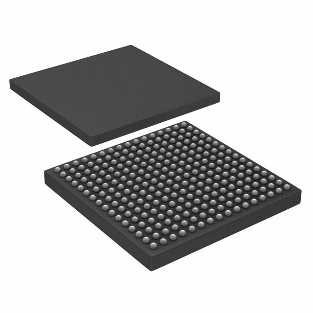
- Part No.:
- VSC8572XKS-04
- Manufacturer:
- Microchip Technology
- Category:
- Telecom
- Package:
- 256-BGA
- Datasheet:
-
 VSC8572XKS-04.pdf
- Description:
- IC TELECOM INTERFACE 256BGA
- Quantity:
- Payment:

- Shipping:

Inventory:4,282
Please send an inquiry. Send us your inquiry, and we will respond immediately.
Product details
Overview
VSC8572XKS-04 from Microsemi (now Microchip) is a dual-port 10/100/1000BASE-T Ethernet PHY IC with integrated IEEE 1588v2 timestamping engine, Synchronous Ethernet support, and QSGMII/SGMII/RGMII MAC interfaces. It delivers sub-50 ns timestamp accuracy, supports one-step and two-step transparent/boundary clock modes, and operates across -40°C to +105°C industrial temperature range. It is deployed in carrier-grade Ethernet switches, precision time-aware industrial controllers, and telecom infrastructure requiring deterministic timing.
For engineers reviewing the VSC8572XKS-04 datasheet, VSC8572XKS-04 pinout, VSC8572XKS-04 application, or VSC8572XKS-04 equivalent, key selection criteria include IEEE 1588 timestamp resolution, SGMII/QSGMII media interface flexibility, Synchronous Ethernet compliance (ITU-T G.8262), PoE support per IEEE 802.3af, and industrial-grade thermal performance.
Technical Context
The VSC8572XKS-04 implements a dual-port PHY with independent SerDes and copper transceivers per port, supporting simultaneous 1000BASE-X fiber and 1000BASE-T copper operation. Its IEEE 1588 timestamping engine includes hardware-accelerated PTP packet parsing, local time counter with 8 ns resolution, and serial timestamp output interface for external TSN synchronization.
Synchronous Ethernet functionality is realized via dual recovered clock outputs (REFCLK1/REFCLK2) with selectable squelch and jitter attenuation, compliant with ITU-T G.8262 EEC Option 1/2. The device supports RGMII timing modes (ID/OD/CD) and configurable GPIOs for link status, interrupt signaling, and LED control.
Key Specifications
| Parameter | Value and Actual Design Meaning |
|---|---|
| Data Rate | 10/100/1000 Mbps per port - supports auto-negotiation and forced mode on copper; 1.25 Gbps SerDes for fiber/SGMII links. |
| IEEE 1588 Accuracy | ±45 ns typical timestamp accuracy - enables sub-microsecond time synchronization in boundary clock applications. |
| Operating Temperature | -40°C to +105°C - qualified for industrial and telecom base station environments without derating. |
| Power Consumption | 1.9 W typical at 1000BASE-T full load - reduced via ActiPHY dynamic power management states. |
| SynchE Compliance | ITU-T G.8262 EEC Option 1 & 2 - provides phase noise and wander performance required for mobile backhaul. |
| MAC Interface | QSGMII/SGMII/RGMII - enables direct connection to multi-core SoCs and FPGAs without external retimers. |
| PoE Support | IEEE 802.3af Class 0–4 detection - allows inline power classification and monitoring on copper ports. |
Pinout & Package
Package: 256-pin 15 mm × 15 mm × 1.0 mm LFBGA (XKS suffix), RoHS-compliant, 0.8 mm pitch.
| Pin/Terminal | Circuit Role | Design Meaning |
|---|---|---|
| REFCLK1_P / REFCLK1_N | Differential reference clock input | Accepts 125 MHz LVDS clock for SGMII/QSGMII timing; used for SynchE master clock recovery. |
| TXD[3:0] / RXD[3:0] | RGMII data bus | Double-data-rate (DDR) interface with programmable delay; supports ID/OD/CD timing modes for FPGA/ASIC alignment. |
| MDIO / MDC | Serial Management Interface | IEEE 802.3 clause 22/45 compliant bus for register access, configuration, and real-time status monitoring. |
| TSO_P / TSO_N | Serial timestamp output | Differential LVDS output carrying hardware-timestamped PTP event messages for external TSN timing units. |
| GPIO[7:0] | Configurable general-purpose I/O | Programmable as inputs/outputs for link status indication, interrupt assertion, or LED control with enhanced serial LED mode. |
Key Features
| Feature | Design Value |
|---|---|
| Hardware IEEE 1588v2 Engine | Full PTP stack offload with one-step/two-step TC/BC/OC modes, Y.1731 OAM delay measurement, and 8 ns local time counter resolution. |
| Synchronous Ethernet Outputs | Dual low-jitter recovered clocks (REFCLK1/REFCLK2) with programmable squelch and G.8262-compliant phase noise profile. |
| Flexible MAC Interface | Single die supports QSGMII (4-lane), SGMII (1-lane), or RGMII (8-bit DDR) - eliminates need for external SerDes or level shifters. |
| ActiPHY Power Management | Three operational states (low-power, wake-up, normal) with <100 µs transition - reduces idle power by >60% vs. legacy PHYs. |
| VeriPHY Cable Diagnostics | On-chip time-domain reflectometry for open/short detection and cable length estimation up to 100 m on Cat5e/6. |
Applications
| Carrier-Grade Metro Switch | Industrial TSN Bridge |
|---|---|
Use Scenario: Aggregation switch in mobile fronthaul/midhaul networks requiring precise time distribution and packet delay measurement. IC Role / Device Role / Timing Role: IEEE 1588 boundary clock with hardware timestamping and SynchE clock recovery for 5G RU/DU synchronization. Use Value: Enables ±50 ns time error budget compliance per ITU-T G.8275.1 while supporting Y.1731 one-way delay measurements on live traffic. |
Use Scenario: Time-Sensitive Networking bridge in factory automation systems with motion control and safety PLCs. IC Role / Device Role / Timing Role: Transparent clock with sub-100 ns residence time and hardware PTP event capture for TSN stream reservation. Use Value: Guarantees deterministic latency under 1 µs per hop and supports IEEE 802.1AS-2020 grandmaster synchronization. |
| Smart Grid Substation Gateway | Defense Communications Router |
Use Scenario: IEC 61850 GOOSE/SV gateway connecting legacy RTUs to modern Ethernet-based protection relays. IC Role / Device Role / Timing Role: IEEE 1588 ordinary clock with IRIG-B input support via GPIO and precise timestamping of sampled values. Use Value: Achieves <1 µs time alignment across IEDs per IEC 61850-9-3, enabling synchronized phasor measurement (PMU). |
Use Scenario: Secure tactical router in airborne or vehicle-mounted C4ISR platforms requiring ruggedized timing and PoE-powered peripherals. IC Role / Device Role / Timing Role: Dual-port PHY with MIL-STD-810G-qualified thermal performance and IEEE 802.3af PoE detection for camera/sensor nodes. Use Value: Maintains 1588 synchronization integrity across shock/vibration events and supports hot-swap PoE peripheral integration. |
Equivalent & Alternatives
The following parts are listed as comparable options for similar Ethernet PHY applications.
| Alternative Part | Technical Difference | Application Difference | Selection Advice |
|---|---|---|---|
| Marvell Alaska 88E1512 | Lacks integrated IEEE 1588 hardware engine; requires external timestamping ASIC or FPGA logic. | Suitable for non-time-critical Gigabit switches where PTP is handled in software or host processor. | Select when cost sensitivity outweighs sub-microsecond timing requirements and SynchE is not needed. |
| Intel Ethernet PHY i210-IS | Single-port only; no QSGMII support; limited to RGMII/SGMII; no SynchE or 1588v2 hardware acceleration. | Targeted at embedded x86 platforms with PCIe-to-ethernet bridges; lacks carrier-grade timing features. | Choose for space-constrained industrial PCs needing basic 1000BASE-T with minimal BOM count. |
Compared with Marvell 88E1512 and Intel i210-IS, the VSC8572XKS-04 uniquely integrates full IEEE 1588v2 hardware timestamping, dual-port SynchE clock recovery, and QSGMII support in a single industrial-temperature package-enabling carrier-class timing without external timing co-processors or retimers.
Availability
VSC8572XKS-04 is available at Aetrix Electronics and suitable for carrier-grade metro switches, industrial TSN bridges, smart grid substations, and defense communications routers requiring stable component supply across extended temperature and long lifecycle commitments.
Supply support for VSC8572XKS-04 includes scheduled delivery planning, volume procurement assistance, BOM continuity management, traceable sourcing, and lifecycle availability coordination for OEM customers, industrial embedded developers, connected-device designers, and electronics production programs.
Manufacturer
Microsemi, now part of Microchip Technology Inc., designs high-reliability semiconductor solutions for aerospace, defense, communications, and industrial markets, with leadership in timing, security, and Ethernet infrastructure.
The VSC8572XKS-04 belongs to Microsemi's Carrier Ethernet PHY product line, engineered specifically for telecom and industrial applications demanding IEEE 1588v2 precision, Synchronous Ethernet compliance, and robust operation in harsh environments.
FAQ
What is the maximum timestamp accuracy achievable with the VSC8572XKS-04 in IEEE 1588 boundary clock mode?
The VSC8572XKS-04 achieves ±45 ns typical timestamp accuracy in IEEE 1588 boundary clock mode under standard operating conditions, verified per IEEE 1588-2008 Annex D test methodology. This accuracy is maintained across its full -40°C to +105°C industrial temperature range and includes compensation for internal SerDes skew and MAC interface delays. The VSC8572XKS-04 uses dedicated hardware timestamp insertion and extraction logic to minimize software-induced jitter, making it suitable for ITU-T G.8275.1-compliant deployments.
Does the VSC8572XKS-04 support both one-step and two-step IEEE 1588 transparent clock operation?
Yes, the VSC8572XKS-04 supports both one-step and two-step IEEE 1588 transparent clock (TC) operation through dedicated hardware timestamping paths and configurable PTP message rewriting logic. Its timestamp processor handles correction field updates in real time for one-step TC, while the rewritable timestamp FIFO and serial timestamp output interface enable precise two-step TC implementation. The VSC8572XKS-04 also supports peer-to-peer TC mode with hardware-assisted delay measurement using Y.1731 OAM frames.
Can the VSC8572XKS-04 operate with RGMII timing modes other than ID (Internal Delay)?
Yes, the VSC8572XKS-04 supports all three RGMII timing modes: ID (Internal Delay), OD (Output Delay), and CD (Clock Delay). Configuration is performed via the RGMII Settings register (Extended Page 2, Address 0x10) and allows system-level alignment with SoC/FPGA RGMII receivers. This flexibility eliminates board-level trace-length matching constraints and enables interoperability with diverse host processors-including Xilinx Zynq, Intel Agilex, and NXP Layerscape devices-without external delay buffers.
Is the VSC8572XKS-04 compatible with IEEE 802.3af PoE powered devices on its copper ports?
Yes, the VSC8572XKS-04 integrates full IEEE 802.3af Class 0–4 PD detection and classification circuitry on both copper ports. It performs signature detection, power classification, and under-voltage lockout per clause 33, enabling safe inline power delivery to connected devices such as IP cameras, wireless APs, and VoIP phones. The VSC8572XKS-04 reports PoE status via MDIO registers and supports GPIO-driven power fault signaling for system-level power management.
What SynchE compliance level does the VSC8572XKS-04 meet, and how is it validated?
The VSC8572XKS-04 meets ITU-T G.8262 EEC Option 1 and Option 2 specifications for Synchronous Ethernet equipment clocks. Validation is based on measured phase noise (≤ –120 dBc/Hz at 12 kHz offset) and wander (TDEV ≤ 5 ns over 1–100 s averaging intervals) of its dual recovered clock outputs (REFCLK1/REFCLK2), as confirmed in Microsemi's compliance report VMDS-10400 Rev 4.3. The VSC8572XKS-04 supports automatic clock selection, squelch control, and holdover mode during reference loss-ensuring continuous SynchE operation in mobile backhaul networks.
VSC8572XKS-04 Specifications
- Product attributes
- Attribute value
- Manufacturer:
- Microchip Technology
- Series:
- -
- Package/Case:
- 256-BGA
- Packaging:
- Tray
- Product Status:
- Obsolete
- Function:
- Ethernet
- Interface:
- RMII
- Number of Circuits:
- 2
- Voltage - Supply:
- 1V, 2.5V
- Current - Supply:
- -
- Power (Watts):
- -
- Operating Temperature:
- -
- Grade:
- -
- Qualification:
- -
- Mounting Type:
- Surface Mount
- Supplier Device Package:
- 256-PBGA (17x17)
VSC8572XKS-04 FAQ
1.How can I place an order for VSC8572XKS-04 through Aetrix?
Please submit a Request for Quotation (RFQ) for VSC8572XKS-04 on Aetrix. Our sales agent will provide a competitive quotation and guide you through the order confirmation once you accept the terms.
2.Are the price and stock information for VSC8572XKS-04 reliable?
The price and inventory of VSC8572XKS-04 are updated periodically and may fluctuate due to market conditions. Stock and pricing data are typically refreshed every 24 hours. Quotation validity for VSC8572XKS-04 is usually 5 days.
3.What payment methods are accepted for VSC8572XKS-04?
We accept Wire Transfer, PayPal, Credit Card, Western Union, MoneyGram, and Escrow for VSC8572XKS-04 transactions.
Note: Certain payment methods may incur a processing fee.
4.How is shipping managed for VSC8572XKS-04?
VSC8572XKS-04 orders can be shipped via leading logistics carriers, including DHL, UPS, FedEx, TNT, or Registered Mail.
Once your VSC8572XKS-04 order is processed, you will receive an email with the shipment details and tracking number.
Note: Tracking information may take up to 24 hours to appear. Express delivery typically takes 3–5 business days.
5.How can I obtain technical support or documentation for VSC8572XKS-04?
For technical support, including VSC8572XKS-04 datasheets, pinout diagrams, or application guidance, please contact our engineering support team. They can provide detailed documentation and assistance for your VSC8572XKS-04 requirements.
6.How does Aetrix verify that VSC8572XKS-04 is sourced from the original manufacturer or authorized distributors?
All VSC8572XKS-04 products on Aetrix are procured from qualified distributors and authorized channels. Our dedicated quality assurance team conducts strict verification, including traceability checks and, if necessary, third-party testing. This ensures that VSC8572XKS-04 meets industry standards.
7.What is the process for return or replacement of VSC8572XKS-04?
All VSC8572XKS-04 units undergo pre-shipment inspection (PSI). If there is an issue with VSC8572XKS-04, returns or replacements are accepted under the following conditions:
1.Quantity discrepancies, incorrect items, or visible external defects (such as breakage or corrosion), acknowledged by Aetrix.
2.The issue is reported within 90 days of delivery.
3.The VSC8572XKS-04 part is unused and in its original packaging.
Return procedure for VSC8572XKS-04:
1.Submit a request within 90 days.
2.Obtain a Return Material Authorization (RMA) from Aetrix.
VSC8572XKS-04 Tags

-
LMC567CMX/NOPB
Texas Instruments
-
LM567CMX/NOPB
Texas Instruments
-
LM567CM/NOPB
Texas Instruments

-
VSC8531XMW-02
Microchip Technology
-
VSC8531XMW-05
Microchip Technology

-
GPY115C0VI
MaxLinear, Inc.

-
SI32185-A-FMR
Skyworks Solutions Inc.

-
VSC8541XMV-05
Microchip Technology

-
SI32178-B-FM1R
Skyworks Solutions Inc.
-
GPY215C0VI
MaxLinear, Inc.

-
CPC7514ZTR
Littelfuse Inc.

-
VSC8502XML-03
Microchip Technology
Tech Hub

TTL and CMOS logic families differ in thresholds, loading, output drive, power and timing. This engineering guide compares 74HC and 74HCT, calculates noise margins and checks 3.3 V/5 V compatibility.

A practical engineering guide to 3.3V and 5V logic compatibility, input thresholds, resistor dividers, translator ICs, MOSFET level shifting, I2C pull-ups, timing limits and power-sequencing risks.

The 74HC595 uses push-pull logic outputs, while the TPIC6B595 uses 50 V open-drain DMOS sinks for higher-power loads. This guide compares timing, current limits, 3.3 V interfacing, load wiring, thermal…

The 74HC595 converts serial data into eight stable parallel outputs. This guide covers pin functions, shift and storage timing, OE and MR behavior, drive-current limits, cascading, voltage compatibilit…

A technical comparison of level-sensitive latches and edge-triggered flip-flops, covering timing windows, setup and hold limits, master–slave operation, time borrowing, race-through, HDL inference and…

A D latch stores one bit while Enable controls when data can pass. This reference covers gate-level operation, truth tables, transparency, setup and hold timing, LE versus OE, common ICs and practical …

An SR latch stores one bit through cross-coupled feedback. This engineering reference covers NOR and NAND implementations, truth tables, forbidden-state recovery, gated operation, switch debouncing, fa…

Latch circuits retain one bit through feedback. This technical reference covers SR and D latches, truth tables, transparency, timing limits, latch-versus-flip-flop behavior, applications and common log…

An engineering guide to LED driver operation, constant-current and constant-voltage outputs, linear and switching topologies, dimming, IC selection, calculations, replacement compatibility, and fault c…

Operational amplifier guide covering op amp basics, feedback, ideal vs real op amps, common configurations, buffer circuits, offset, bias current, gain-bandwidth, slew rate, rail-to-rail limits and sel…


