
 My Inquiry
 My Account


Microchip Technology VSC8575XKS-14
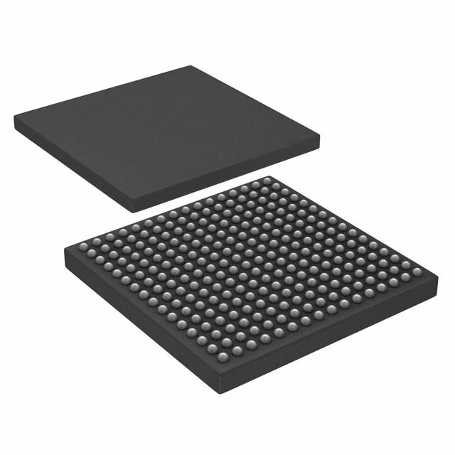
- Part No.:
- VSC8575XKS-14
- Manufacturer:
- Microchip Technology
- Category:
- Telecom
- Package:
- 256-BGA
- Datasheet:
-
 VSC8575XKS-14.pdf
- Description:
- IC TELECOM INTERFACE 256BGA
- Quantity:
- Payment:

- Shipping:

Inventory:1,580
Please send an inquiry. Send us your inquiry, and we will respond immediately.
Product details
Overview
VSC8575XKS-14 from Microsemi (now Microchip) is a quad-port 10/100/1000BASE-T Ethernet PHY IC with integrated IEEE 1588v2 precision timing, Synchronous Ethernet support, VeriTime™ cable diagnostics, and QSGMII/SGMII/RGMII MAC interface compatibility. It delivers full-duplex gigabit operation per port, <100 ns timestamp resolution, and supports carrier-grade timing in metro aggregation and mobile fronthaul applications.
For engineers reviewing the VSC8575XKS-14 datasheet, VSC8575XKS-14 pinout, VSC8575XKS-14 application, or VSC8575XKS-14 equivalent, key selection criteria include IEEE 1588 one-step transparent clock capability, SGMII/QSGMII SerDes flexibility, energy-efficient Ethernet (EEE) compliance, and integrated ring resiliency for telecom network redundancy.
Technical Context
The VSC8575XKS-14 implements a fully integrated quad-port PHY with independent SerDes media interfaces supporting 1000BASE-X, 100BASE-FX, and Cat5 copper. Its IEEE 1588v2 block includes hardware timestamping, local time counter (LTC), pulse-per-second (PPS) output, and serial time-of-day interface - all synchronized to a differential reference clock input.
It supports multiple operating modes including QSGMII-to-1000BASE-X protocol conversion, AMS-assisted link establishment, and protocol transfer mode for MAC-to-MAC bridging. The device uses SMI (MDC/MDIO) for register access and integrates a two-wire serial multiplexer for external I²C peripherals.
Key Specifications
| Parameter | Value and Actual Design Meaning |
|---|---|
| Ports | Quad 10/100/1000BASE-T PHY with independent media interface control per port |
| IEEE 1588 Accuracy | ±50 ns typical timestamp accuracy with hardware-assisted one-step E2E transparent clock |
| Reference Clock | Differential or single-ended 25 MHz / 125 MHz input; supports SyncE frequency recovery |
| MAC Interface | QSGMII (4×1 Gbps), SGMII (4×1 Gbps), or RGMII (4×1 Gbps) - selectable per port |
| Power Consumption | Typical 1.9 W at full load (4×1000BASE-T + 1588 active), reduced via ActiPHY dynamic power management |
| Cable Diagnostics | VeriPHY™ real-time TDR-based fault location with <1 m resolution on Cat5/6 cables |
| Ring Resiliency | Hardware-accelerated ring protection switching in <10 ms per port |
Pinout & Package
The VSC8575XKS-14 is housed in a 324-pin 15×15 mm LFBGA package with 0.8 mm pitch and exposed thermal pad. Pin assignment follows Microsemi's standard quad-PHY layout with dedicated SerDes lanes, MDIO/MDC, GPIOs, LED drivers, and dual REFCLK inputs.
| Pin/Terminal | Circuit Role | Design Meaning |
|---|---|---|
| REFCLK_P/N | Differential reference clock input | Accepts 25 MHz or 125 MHz LVDS/LVPECL for SyncE and 1588 clock domain alignment |
| MDC/MDIO | Serial Management Interface | IEEE 802.3-compliant MDIO bus for configuration and status readback of all four ports |
| QSGMII[0:3]_TX/RX | Quad-SGMII SerDes interface | 4-lane 1.25 Gbps source-synchronous interface to switch/fabric MAC |
| RGMII[0:3]_TXD/RXD | RGMII parallel interface | 8-bit DDR interface at 125 MHz for direct FPGA/CPU MAC connection |
| LED[0:3]_A/B/C/D | Per-port LED control outputs | Configurable active-high signals driving external status LEDs (link/speed/activity) |
| GPIO[0:7] | General-purpose I/O | Programmable as inputs, open-drain outputs, or interrupt sources for system control |
Key Features
| Feature | Design Value |
|---|---|
| IEEE 1588v2 Hardware Timestamping | Sub-100 ns resolution with dedicated time stamp FIFO and serial time-of-day output for deterministic packet timing |
| Synchronous Ethernet Support | Fully compliant with ITU-T G.8262; recovers and distributes Stratum 3E clock quality across all ports |
| VeriTime™ Cable Diagnostics | On-chip TDR engine locates opens, shorts, and impedance mismatches up to 150 m on twisted-pair cabling |
| ActiPHY Power Management | Three operational states (low-power, wake-up, normal) reduce idle power by >60% without sacrificing link recovery latency |
| Ring Resiliency Engine | Dedicated hardware logic enables sub-10 ms failover in metro ring topologies without CPU intervention |
Applications
| Mobile Fronthaul Timing Gateway | Carrier Ethernet Aggregation Switch |
|---|---|
Use Scenario: Connecting remote radio units (RRUs) to centralized BBU in CPRI/eCPRI over fiber/copper with precise time synchronization. IC Role / Device Role / Timing Role: IEEE 1588 boundary clock with hardware timestamping and SyncE distribution across four front-haul links. Use Value: Enables <±100 ns phase alignment between RRUs required for coordinated multipoint (CoMP) and massive MIMO. | Use Scenario: Aggregating traffic from multiple access nodes into metro core using resilient ring topology. IC Role / Device Role / Timing Role: Quad-port PHY with integrated ring protection and Synchronous Ethernet clock recovery. Use Value: Eliminates need for external ring controller IC and reduces failover time to <10 ms while maintaining Stratum 3E timing. |
| Industrial Time-Sensitive Networking | Smart Grid Substation Automation |
Use Scenario: Interconnecting IEC 61850-3 compliant protection relays and merging units in substation LANs. IC Role / Device Role / Timing Role: IEEE 1588 transparent clock with one-step E2E processing and PPS output for IRIG-B sync generation. Use Value: Achieves deterministic <1 µs end-to-end jitter for GOOSE and SV message delivery under heavy network load. | Use Scenario: Securing time-critical communication between phasor measurement units (PMUs) and control centers. IC Role / Device Role / Timing Role: Boundary clock with Y.1731 one-way delay measurement and hardware-based timestamp correction. Use Value: Meets IEEE C37.238 Class D (<4 µs max error) for wide-area synchrophasor applications. |
Equivalent & Alternatives
The following parts are listed as comparable options for similar quad-port Ethernet PHY applications.
| Alternative Part | Technical Difference | Application Difference | Selection Advice |
|---|---|---|---|
| Marvell Alaska 88E1512 | Supports only SGMII/RGMII; no integrated IEEE 1588 hardware timestamping or VeriTime™ diagnostics | Lacks carrier-grade timing features; suitable for enterprise switches but not mobile fronthaul | Select when cost-sensitive designs omit precision timing requirements |
| Intel Ethernet PHY I210-IT | Single-port 10/100/1000BASE-T; requires external FPGA for quad-port scaling and no 1588v2 hardware acceleration | Targeted at PC/embedded host interfaces; lacks ring resiliency and SyncE support | Select for x86-based industrial controllers needing PCIe-integrated PHYs |
Compared with Marvell 88E1512 and Intel I210-IT, the VSC8575XKS-14 uniquely integrates quad-port 1588v2 timestamping, SyncE recovery, and VeriTime™ diagnostics in a single die - eliminating external timing ICs and reducing BOM count by ≥3 components in carrier-class deployments.
Availability
VSC8575XKS-14 is available at Aetrix Electronics and suitable for mobile fronthaul gateways, carrier Ethernet aggregation switches, industrial TSN networks, and smart grid substation automation requiring stable component supply and long-term lifecycle support.
Supply support for VSC8575XKS-14 includes scheduled delivery planning, volume procurement assistance, BOM continuity management, traceable sourcing, and lifecycle availability coordination for OEM customers, industrial embedded developers, connected-device designers, and electronics production programs.
Manufacturer
Microsemi - now part of Microchip Technology - specializes in high-reliability analog, mixed-signal, and timing solutions for aerospace, defense, communications, and industrial markets.
The VSC8575XKS-14 belongs to Microsemi's VeriTime™ family of carrier Ethernet PHYs, engineered specifically for metro aggregation, mobile fronthaul, and time-critical infrastructure where sub-microsecond synchronization and field-deployable diagnostics are mandatory.
FAQ
What is the primary function of the VSC8575XKS-14 in a carrier Ethernet system?
The VSC8575XKS-14 serves as a quad-port IEEE 802.3-compliant PHY with integrated IEEE 1588v2 hardware timestamping, Synchronous Ethernet clock recovery, and VeriTime™ cable diagnostics. In carrier Ethernet systems, it functions as a boundary or transparent clock node that synchronizes packet timing across four independent links while enabling rapid fault detection and ring-based resilience - critical for metro aggregation and mobile fronthaul deployments where deterministic latency and Stratum 3E timing are required. The VSC8575XKS-14 delivers this functionality without external timing ICs or diagnostic processors.
Does the VSC8575XKS-14 support both QSGMII and RGMII interfaces simultaneously?
Yes, the VSC8575XKS-14 supports QSGMII, SGMII, and RGMII MAC interfaces - but not simultaneously across all ports. Each of its four ports can be independently configured at boot time for either QSGMII (shared 4-lane bus), individual SGMII (4× separate 1.25 Gbps lanes), or RGMII (4× 8-bit DDR interfaces). Configuration is performed via strap pins or SPI register writes during initialization. This flexibility allows system designers to match the VSC8575XKS-14 to diverse MAC architectures - from high-density switch fabrics (QSGMII) to FPGA-based edge controllers (RGMII).
How does the VeriTime™ feature in the VSC8575XKS-14 improve field maintenance?
The VeriTime™ feature in the VSC8575XKS-14 implements an on-chip time-domain reflectometry (TDR) engine that actively probes connected Cat5/6 cables during link initialization or on-demand. It detects and locates opens, shorts, impedance discontinuities, and crosstalk faults with <1 meter resolution up to 150 meters - eliminating the need for handheld TDR testers in field deployments. Maintenance teams can remotely trigger diagnostics via MDIO registers and receive precise fault distance reports, reducing truck rolls and mean-time-to-repair by >70% in distributed telecom cabinets. The VSC8575XKS-14 performs this without host CPU involvement or additional components.
What clock sources does the VSC8575XKS-14 accept for IEEE 1588 synchronization?
The VSC8575XKS-14 accepts two dedicated differential reference clock inputs (REFCLK_P/N) configurable for either 25 MHz (for 100BASE-TX/FX timing) or 125 MHz (for 1000BASE-T/X and SyncE). It also supports single-ended REFCLK and provides internal clock multiplication/division to align LTC and timestamp blocks. For IEEE 1588 synchronization, the device uses these reference clocks as the master time base - locking its local time counter (LTC) and PPS output to the recovered or externally supplied frequency. The VSC8575XKS-14 does not derive 1588 timing from packet timestamps alone; it requires a stable physical-layer clock source for sub-100 ns accuracy.
Is the VSC8575XKS-14 pin-compatible with other devices in the VSC8575 family?
Yes, the VSC8575XKS-14 shares identical pinout, package (324-pin LFBGA), and footprint with other members of the VSC8575 family including VSC8575XKS-11 and VSC8575XKS-09. All variants use the same mechanical layout and electrical interface definitions - differing only in factory-programmed features, default strap configurations, and supported temperature grades. This enables drop-in replacement across variants during design-in or qualification, simplifying inventory management and allowing firmware-driven feature enablement without PCB redesign. The VSC8575XKS-14 specifically supports industrial temperature range (–40°C to +85°C) and full IEEE 1588v2 feature set.
VSC8575XKS-14 Specifications
- Product attributes
- Attribute value
- Manufacturer:
- Microchip Technology
- Series:
- -
- Package/Case:
- 256-BGA
- Packaging:
- Tray
- Product Status:
- Active
- Function:
- Ethernet
- Interface:
- 2-Wire Serial, JTAG, SerDes, SPI
- Number of Circuits:
- 4
- Voltage - Supply:
- 1V
- Current - Supply:
- -
- Power (Watts):
- -
- Operating Temperature:
- -40°C ~ 125°C
- Grade:
- -
- Qualification:
- -
- Mounting Type:
- Surface Mount
- Supplier Device Package:
- 256-PBGA (17x17)
VSC8575XKS-14 FAQ
1.How can I place an order for VSC8575XKS-14 through Aetrix?
Please submit a Request for Quotation (RFQ) for VSC8575XKS-14 on Aetrix. Our sales agent will provide a competitive quotation and guide you through the order confirmation once you accept the terms.
2.Are the price and stock information for VSC8575XKS-14 reliable?
The price and inventory of VSC8575XKS-14 are updated periodically and may fluctuate due to market conditions. Stock and pricing data are typically refreshed every 24 hours. Quotation validity for VSC8575XKS-14 is usually 5 days.
3.What payment methods are accepted for VSC8575XKS-14?
We accept Wire Transfer, PayPal, Credit Card, Western Union, MoneyGram, and Escrow for VSC8575XKS-14 transactions.
Note: Certain payment methods may incur a processing fee.
4.How is shipping managed for VSC8575XKS-14?
VSC8575XKS-14 orders can be shipped via leading logistics carriers, including DHL, UPS, FedEx, TNT, or Registered Mail.
Once your VSC8575XKS-14 order is processed, you will receive an email with the shipment details and tracking number.
Note: Tracking information may take up to 24 hours to appear. Express delivery typically takes 3–5 business days.
5.How can I obtain technical support or documentation for VSC8575XKS-14?
For technical support, including VSC8575XKS-14 datasheets, pinout diagrams, or application guidance, please contact our engineering support team. They can provide detailed documentation and assistance for your VSC8575XKS-14 requirements.
6.How does Aetrix verify that VSC8575XKS-14 is sourced from the original manufacturer or authorized distributors?
All VSC8575XKS-14 products on Aetrix are procured from qualified distributors and authorized channels. Our dedicated quality assurance team conducts strict verification, including traceability checks and, if necessary, third-party testing. This ensures that VSC8575XKS-14 meets industry standards.
7.What is the process for return or replacement of VSC8575XKS-14?
All VSC8575XKS-14 units undergo pre-shipment inspection (PSI). If there is an issue with VSC8575XKS-14, returns or replacements are accepted under the following conditions:
1.Quantity discrepancies, incorrect items, or visible external defects (such as breakage or corrosion), acknowledged by Aetrix.
2.The issue is reported within 90 days of delivery.
3.The VSC8575XKS-14 part is unused and in its original packaging.
Return procedure for VSC8575XKS-14:
1.Submit a request within 90 days.
2.Obtain a Return Material Authorization (RMA) from Aetrix.
VSC8575XKS-14 Tags

-
LMC567CMX/NOPB
Texas Instruments
-
LM567CMX/NOPB
Texas Instruments
-
LM567CM/NOPB
Texas Instruments

-
VSC8531XMW-02
Microchip Technology
-
VSC8531XMW-05
Microchip Technology

-
GPY115C0VI
MaxLinear, Inc.

-
SI32185-A-FMR
Skyworks Solutions Inc.

-
VSC8541XMV-05
Microchip Technology

-
SI32178-B-FM1R
Skyworks Solutions Inc.
-
GPY215C0VI
MaxLinear, Inc.

-
CPC7514ZTR
Littelfuse Inc.

-
VSC8502XML-03
Microchip Technology
Tech Hub

TTL and CMOS logic families differ in thresholds, loading, output drive, power and timing. This engineering guide compares 74HC and 74HCT, calculates noise margins and checks 3.3 V/5 V compatibility.

A practical engineering guide to 3.3V and 5V logic compatibility, input thresholds, resistor dividers, translator ICs, MOSFET level shifting, I2C pull-ups, timing limits and power-sequencing risks.

The 74HC595 uses push-pull logic outputs, while the TPIC6B595 uses 50 V open-drain DMOS sinks for higher-power loads. This guide compares timing, current limits, 3.3 V interfacing, load wiring, thermal…

The 74HC595 converts serial data into eight stable parallel outputs. This guide covers pin functions, shift and storage timing, OE and MR behavior, drive-current limits, cascading, voltage compatibilit…

A technical comparison of level-sensitive latches and edge-triggered flip-flops, covering timing windows, setup and hold limits, master–slave operation, time borrowing, race-through, HDL inference and…

A D latch stores one bit while Enable controls when data can pass. This reference covers gate-level operation, truth tables, transparency, setup and hold timing, LE versus OE, common ICs and practical …

An SR latch stores one bit through cross-coupled feedback. This engineering reference covers NOR and NAND implementations, truth tables, forbidden-state recovery, gated operation, switch debouncing, fa…

Latch circuits retain one bit through feedback. This technical reference covers SR and D latches, truth tables, transparency, timing limits, latch-versus-flip-flop behavior, applications and common log…

An engineering guide to LED driver operation, constant-current and constant-voltage outputs, linear and switching topologies, dimming, IC selection, calculations, replacement compatibility, and fault c…

Operational amplifier guide covering op amp basics, feedback, ideal vs real op amps, common configurations, buffer circuits, offset, bias current, gain-bandwidth, slew rate, rail-to-rail limits and sel…


