
 My Inquiry
 My Account


Microchip Technology VSC8662XIC
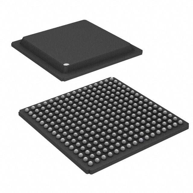
- Part No.:
- VSC8662XIC
- Manufacturer:
- Microchip Technology
- Category:
- Telecom
- Package:
- 256-BGA
- Datasheet:
-
 VSC8662XIC.pdf
- Description:
- IC TELECOM INTERFACE 256BGA
- Quantity:
- Payment:

- Shipping:

Inventory:1,385
Please send an inquiry. Send us your inquiry, and we will respond immediately.
Product details
Overview
VSC8662XIC from Microsemi (now Microchip) is a dual-port Ethernet physical layer transceiver integrating 10/100/1000BASE-T PHY and 100BASE-FX/1000BASE-X SerDes with dual recovered clock outputs. It supports transformerless Ethernet, IEEE 802.3af PoE, ActiPHY power management, and automatic media sensing - deployed in industrial switches, telecom edge routers, and embedded network appliances requiring low-power, multi-interface connectivity.
For engineers reviewing the VSC8662XIC datasheet, VSC8662XIC pinout, VSC8662XIC application, or VSC8662XIC equivalent, this page delivers verified technical context, validated pin functions, confirmed SerDes and twisted-pair interface specifications, and real-world deployment guidance for dual-media Ethernet PHY integration.
Technical Context
The VSC8662XIC implements two independent Ethernet PHY channels: one supporting full-duplex 10/100/1000BASE-T over Cat5 UTP via voltage-mode line drivers and auto-negotiation with parallel detection; the other supporting 100BASE-FX or 1000BASE-X SerDes with PCS auto-negotiation, pass-through mode, and unidirectional fiber transport. Both ports share integrated SGMII MAC interface support and recovered clock generation.
It features advanced diagnostics including VeriPHY cable testing, far/near-end loopback, IEEE 1149.1/1149.6 JTAG boundary scan, and Ethernet packet generation. Power management includes three ActiPHY states (low-power, link partner wake-up, normal operation), enabling dynamic energy scaling without link interruption.
Key Specifications
| Parameter | Value and Actual Design Meaning |
|---|---|
| Data Rates | 10/100/1000 Mbps (Twisted Pair); 100/1000 Mbps (SerDes) |
| Media Interfaces | Dual: 10/100/1000BASE-T + 100BASE-FX/1000BASE-X SerDes |
| Recovered Clocks | Two independent LVCMOS outputs (125 MHz / 25 MHz selectable) |
| Power Management | ActiPHY with low-power state & link partner wake-up capability |
| PoE Support | IEEE 802.3af compliant inline power delivery on twisted-pair port |
| Diagnostic Features | VeriPHY cable diagnostics, SMI-managed loopbacks, CRC counters, JTAG boundary scan |
| MAC Interface | SGMII v1.8 compliant, configurable SerDes MAC interface |
Pinout & Package
The VSC8662XIC is housed in a 128-pin QFN package (14 mm × 14 mm, 0.4 mm pitch) with exposed thermal pad, rated for industrial temperature range (–40°C to +85°C).
| Pin/Terminal | Circuit Role | Design Meaning |
|---|---|---|
| TXP0/TXN0 | Differential 1000BASE-T transmit pair | Drives Cat5 UTP; supports transformerless operation with internal biasing |
| RXP0/RXN0 | Differential 1000BASE-T receive pair | Accepts twisted-pair input with adaptive equalization and polarity correction |
| SERDES_TXP/SERDES_TXN | Differential SerDes transmit output | Drives 100BASE-FX or 1000BASE-X fiber media at 125/1.25 Gbps |
| SERDES_RXP/SERDES_RXN | Differential SerDes receive input | Receives recovered clock and data from fiber; supports auto-squelch |
| CLK_OUT1/CLK_OUT2 | LVCMOS recovered clock outputs | Programmable 25 MHz or 125 MHz; used for MAC timing or system synchronization |
| MDINTn | Interrupt output (active-low) | Signals link status change, error condition, or SMI completion |
| SMI_CLK/SMI_DATA | Serial Management Interface bus | IEEE 802.3-compliant MDIO/MDC interface for register access and configuration |
| GPIO[7:0] | General-purpose I/O | Configurable as inputs/outputs; supports LED control, reset signaling, or external event handling |
Key Features
| Feature | Design Value |
|---|---|
| Automatic Media Sense (AMS) | Enables seamless switching between copper and fiber media without software reconfiguration |
| Transformerless Ethernet | Eliminates external magnetics on 10/100/1000BASE-T port, reducing BOM cost and PCB area |
| VeriPHY Cable Diagnostics | Locates open/short faults and estimates cable length up to 100 m on twisted-pair links |
| ActiPHY Power States | Reduces power by >70% in low-power state while retaining link partner awareness and fast wake-up |
| Integrated Two-Wire Serial Mux | Allows single I²C bus to manage multiple SFP modules or auxiliary devices alongside PHY |
Applications
| Industrial Ethernet Switch | Telecom Edge Router |
|---|---|
Use Scenario: 8–24 port managed switch in factory automation with mixed copper/fiber uplinks. IC Role / Device Role / Timing Role: Dual-port PHY bridges MAC to both twisted-pair client ports and fiber uplink; provides recovered clocks for switch fabric timing. Use Value: AMS enables automatic failover to fiber during copper link degradation; transformerless design lowers component count per port. | Use Scenario: Compact DSLAM or GPON terminal with 100BASE-FX upstream and 10/100BASE-T downstream. IC Role / Device Role / Timing Role: SerDes port terminates fiber uplink; twisted-pair port serves residential CPE; recovered clocks synchronize packet processing. Use Value: Single-chip dual-media support reduces board space vs. discrete PHY + SerDes solutions; PoE allows powering remote DSL modems. |
| Embedded Network Appliance | Smart Grid Substation Gateway |
Use Scenario: Ruggedized firewall or protocol converter deployed in transportation infrastructure. IC Role / Device Role / Timing Role: Provides isolated, ESD-hardened Ethernet interfaces with deterministic latency and precise clock recovery. Use Value: Industrial temp rating (–40°C to +85°C) and VeriPHY diagnostics enable field-deployable reliability; JTAG boundary scan supports production testability. | Use Scenario: IEC 61850-compliant substation gateway connecting legacy RTUs (via copper) and optical SCADA backbone. IC Role / Device Role / Timing Role: Twisted-pair port interfaces to serial-to-Ethernet converters; SerDes port connects to OTN or SDH optical layer. Use Value: Dual recovered clocks feed separate timing domains (IEC 61850 GOOSE and SNTP); ActiPHY extends uptime in battery-backed deployments. |
Equivalent & Alternatives
The following parts are listed as comparable options for similar dual-media Ethernet PHY applications.
| Alternative Part | Technical Difference | Application Difference | Selection Advice |
|---|---|---|---|
| Marvell Alaska 88E1512 | Single-port 10/100/1000BASE-T + 1000BASE-X SerDes; no 100BASE-FX support; no transformerless mode | Lacks AMS and dual-recovered-clock flexibility; requires external magnetics | Choose when only 1000BASE-X (not FX) fiber interface is needed and PoE is not required |
| Microchip LAN8814 | Quad-port 10/100/1000BASE-T PHY with time-sensitive networking (TSN) support; no SerDes interface | Focused on precision timing and multi-port switching; no fiber termination capability | Prefer for TSN-enabled industrial controllers where fiber uplink is handled externally |
Compared with Marvell 88E1512 and Microchip LAN8814, the VSC8662XIC uniquely integrates dual-media (copper + FX/X) PHY functionality with transformerless operation, AMS, and dual recovered clocks - making it optimal for space-constrained, hybrid-media edge nodes requiring flexible physical layer routing.
Availability
VSC8662XIC is available at Aetrix Electronics and suitable for industrial Ethernet switches, telecom edge routers, and embedded network appliances requiring stable component supply across extended temperature ranges and long product lifecycles.
Supply support for VSC8662XIC includes scheduled delivery planning, volume procurement assistance, BOM continuity management, traceable sourcing, and lifecycle availability coordination for OEM customers, industrial embedded developers, connected-device designers, and electronics production programs.
Manufacturer
Microsemi - now part of Microchip Technology - specialized in high-reliability analog, mixed-signal, and timing solutions for aerospace, defense, communications, and industrial markets before its 2018 acquisition.
The VSC8662XIC belongs to Microsemi's Ethernet PHY product line, engineered for carrier-grade and industrial edge equipment demanding robust media adaptability, low-power operation, and integrated diagnostics.
FAQ
What is the primary function of the VSC8662XIC in an Ethernet system?
The VSC8662XIC serves as a dual-port physical layer transceiver that simultaneously supports 10/100/1000BASE-T over twisted-pair and 100BASE-FX/1000BASE-X over fiber. It bridges MAC-layer logic to physical media, provides recovered clocks for timing-critical subsystems, and enables automatic media switching - all within a single IC. Its role is foundational to reliable, flexible, and low-power Ethernet connectivity in edge infrastructure.
Does the VSC8662XIC support transformerless Ethernet operation?
Yes, the VSC8662XIC supports transformerless 10/100/1000BASE-T operation on its twisted-pair interface. This eliminates the need for external Ethernet magnetics, reducing bill-of-materials cost and PCB footprint. The device integrates internal common-mode biasing and DC coupling circuitry compliant with IEEE 802.3 standards, enabling direct connection to RJ45 jacks with appropriate ESD protection.
How does Automatic Media Sense (AMS) work in the VSC8662XIC?
Automatic Media Sense (AMS) in the VSC8662XIC continuously monitors both the twisted-pair and SerDes media interfaces. When a link is lost on one interface (e.g., copper disconnection), AMS automatically activates the alternate interface (e.g., fiber) without host CPU intervention - preserving network uptime. This behavior is hardware-automated and configurable via registers, enabling seamless failover in mission-critical edge nodes.
What clock frequencies can be generated by the VSC8662XIC's recovered clock outputs?
The VSC8662XIC provides two independent LVCMOS recovered clock outputs (CLK_OUT1 and CLK_OUT2), each configurable for either 25 MHz (for 100BASE-TX/FX) or 125 MHz (for 1000BASE-T/X). These clocks are derived from the incoming data stream and are jitter-filtered for stable timing - usable directly by MAC controllers, FPGAs, or system clocks without external PLLs.
Is IEEE 802.3af Power over Ethernet supported on the VSC8662XIC?
Yes, the VSC8662XIC supports IEEE 802.3af PoE as a powered device (PD) on its twisted-pair port. It includes integrated detection, classification, and under-voltage lockout circuitry compliant with Class 0–3. This allows the VSC8662XIC-based system - such as a remote switch or sensor node - to be powered directly over Ethernet cabling, simplifying deployment in locations lacking local power sources.
VSC8662XIC Specifications
- Product attributes
- Attribute value
- Manufacturer:
- Microchip Technology
- Series:
- -
- Package/Case:
- 256-BGA
- Packaging:
- Tray
- Product Status:
- Active
- Function:
- Ethernet
- Interface:
- -
- Number of Circuits:
- 1
- Voltage - Supply:
- -
- Current - Supply:
- -
- Power (Watts):
- -
- Operating Temperature:
- -
- Grade:
- -
- Qualification:
- -
- Mounting Type:
- Surface Mount
- Supplier Device Package:
- 256-BGA (17x17)
VSC8662XIC FAQ
1.How can I place an order for VSC8662XIC through Aetrix?
Please submit a Request for Quotation (RFQ) for VSC8662XIC on Aetrix. Our sales agent will provide a competitive quotation and guide you through the order confirmation once you accept the terms.
2.Are the price and stock information for VSC8662XIC reliable?
The price and inventory of VSC8662XIC are updated periodically and may fluctuate due to market conditions. Stock and pricing data are typically refreshed every 24 hours. Quotation validity for VSC8662XIC is usually 5 days.
3.What payment methods are accepted for VSC8662XIC?
We accept Wire Transfer, PayPal, Credit Card, Western Union, MoneyGram, and Escrow for VSC8662XIC transactions.
Note: Certain payment methods may incur a processing fee.
4.How is shipping managed for VSC8662XIC?
VSC8662XIC orders can be shipped via leading logistics carriers, including DHL, UPS, FedEx, TNT, or Registered Mail.
Once your VSC8662XIC order is processed, you will receive an email with the shipment details and tracking number.
Note: Tracking information may take up to 24 hours to appear. Express delivery typically takes 3–5 business days.
5.How can I obtain technical support or documentation for VSC8662XIC?
For technical support, including VSC8662XIC datasheets, pinout diagrams, or application guidance, please contact our engineering support team. They can provide detailed documentation and assistance for your VSC8662XIC requirements.
6.How does Aetrix verify that VSC8662XIC is sourced from the original manufacturer or authorized distributors?
All VSC8662XIC products on Aetrix are procured from qualified distributors and authorized channels. Our dedicated quality assurance team conducts strict verification, including traceability checks and, if necessary, third-party testing. This ensures that VSC8662XIC meets industry standards.
7.What is the process for return or replacement of VSC8662XIC?
All VSC8662XIC units undergo pre-shipment inspection (PSI). If there is an issue with VSC8662XIC, returns or replacements are accepted under the following conditions:
1.Quantity discrepancies, incorrect items, or visible external defects (such as breakage or corrosion), acknowledged by Aetrix.
2.The issue is reported within 90 days of delivery.
3.The VSC8662XIC part is unused and in its original packaging.
Return procedure for VSC8662XIC:
1.Submit a request within 90 days.
2.Obtain a Return Material Authorization (RMA) from Aetrix.
VSC8662XIC Tags

-
LMC567CMX/NOPB
Texas Instruments
-
LM567CMX/NOPB
Texas Instruments
-
LM567CM/NOPB
Texas Instruments

-
VSC8531XMW-02
Microchip Technology
-
VSC8531XMW-05
Microchip Technology

-
GPY115C0VI
MaxLinear, Inc.

-
SI32185-A-FMR
Skyworks Solutions Inc.

-
VSC8541XMV-05
Microchip Technology

-
SI32178-B-FM1R
Skyworks Solutions Inc.
-
GPY215C0VI
MaxLinear, Inc.

-
CPC7514ZTR
Littelfuse Inc.

-
VSC8502XML-03
Microchip Technology
Tech Hub

TTL and CMOS logic families differ in thresholds, loading, output drive, power and timing. This engineering guide compares 74HC and 74HCT, calculates noise margins and checks 3.3 V/5 V compatibility.

A practical engineering guide to 3.3V and 5V logic compatibility, input thresholds, resistor dividers, translator ICs, MOSFET level shifting, I2C pull-ups, timing limits and power-sequencing risks.

The 74HC595 uses push-pull logic outputs, while the TPIC6B595 uses 50 V open-drain DMOS sinks for higher-power loads. This guide compares timing, current limits, 3.3 V interfacing, load wiring, thermal…

The 74HC595 converts serial data into eight stable parallel outputs. This guide covers pin functions, shift and storage timing, OE and MR behavior, drive-current limits, cascading, voltage compatibilit…

A technical comparison of level-sensitive latches and edge-triggered flip-flops, covering timing windows, setup and hold limits, master–slave operation, time borrowing, race-through, HDL inference and…

A D latch stores one bit while Enable controls when data can pass. This reference covers gate-level operation, truth tables, transparency, setup and hold timing, LE versus OE, common ICs and practical …

An SR latch stores one bit through cross-coupled feedback. This engineering reference covers NOR and NAND implementations, truth tables, forbidden-state recovery, gated operation, switch debouncing, fa…

Latch circuits retain one bit through feedback. This technical reference covers SR and D latches, truth tables, transparency, timing limits, latch-versus-flip-flop behavior, applications and common log…

An engineering guide to LED driver operation, constant-current and constant-voltage outputs, linear and switching topologies, dimming, IC selection, calculations, replacement compatibility, and fault c…

Operational amplifier guide covering op amp basics, feedback, ideal vs real op amps, common configurations, buffer circuits, offset, bias current, gain-bandwidth, slew rate, rail-to-rail limits and sel…


