
 My Inquiry
 My Account


Texas Instruments VSP2264GSJ
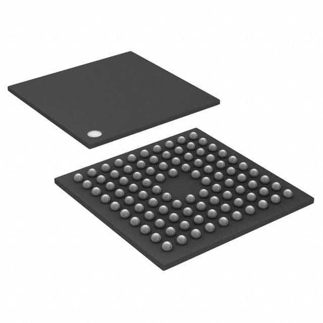
- Part No.:
- VSP2264GSJ
- Manufacturer:
- Texas Instruments
- Category:
- Video Processing
- Package:
- 96-TFBGA
- Datasheet:
-
 VSP2264GSJ.pdf
- Description:
- IC VIDEO CCD SIGNAL PROC 96BGA
- Quantity:
- Payment:

- Shipping:

Inventory:2,438
Please send an inquiry. Send us your inquiry, and we will respond immediately.
Product details
Overview
VSP2264GSJ from Texas Instruments is a mixed-signal CCD signal processor IC integrating a timing generator, 14-bit ADC, correlated double sampler (CDS), and digital programmable-gain amplifier (PGA). It delivers –6 dB to 42 dB gain control, 79 dB SNR, and supports up to 25-MHz conversion rate for high-resolution digital still camera (DSC) image acquisition systems using Panasonic MN39594 or compatible CCD sensors.
For engineers reviewing the VSP2264GSJ datasheet, VSP2264GSJ pinout, VSP2264GSJ application, or VSP2264GSJ equivalent, key selection criteria include vertical/horizontal timing programmability (0.6 ns fine phase step), black-level clamping accuracy, CDS offset adjustment, and low-power operation modes (6 mW MCLK-off, 39 mW standby+power-save).
Technical Context
The VSP2264GSJ integrates a dual-domain timing generator supporting both pixel-rate (H-rate) and line-rate (V-rate) timing synthesis for CCD sensors. Its H-rate block generates six high-speed pulses (R, H1, HL/H2, SHP, SHD, ADCCK) with 16-step phase adjustment (0.6 ns minimum step); V-rate generation uses 11-bit line and 13-bit pixel counters enabling up to 2047 lines × 4095 pixels per frame.
The analog front end includes a switched-capacitor CDS with external coupling (0.1 µF CIN), input clamp referenced to CM = 1.5 V, 14-bit pipelined ADC with full-scale linearity, and a digital PGA with linear-in-dB gain curve. Black-level clamping uses an internal 10-bit DAC and optical black (OB) level sampling via COB terminal.
Key Specifications
| Parameter | Value and Actual Design Meaning |
|---|---|
| ADC Resolution | 14-bit - provides full-scale dynamic range without missing codes at ≤25 MHz conversion rate |
| PGA Gain Range | –6 dB to 42 dB - digitally programmable in linear-dB steps for precise exposure control |
| Signal-to-Noise Ratio | 79 dB - measured at 20 MHz, 3.0 V supply, enabling high-fidelity image digitization |
| Power Consumption | 130 mW active / 39 mW standby+power-save / 6 mW MCLK-off - supports portable DSC battery life optimization |
| Timing Precision | 0.6 ns fine-phase step on SHP/SHD/ADCCK - enables sub-pixel CCD clock alignment for reduced smear |
| Supply Voltage | 3.0 V to 3.6 V - single-supply operation compatible with low-voltage system rails |
| Operating Temperature | –25°C to +85°C - qualified for industrial and consumer camera module environments |
Pinout & Package
Package: 96-ball BGA (GSJ package code), 0.8 mm pitch, 10 mm × 10 mm body size, RoHS-compliant.
| Pin/Terminal | Circuit Role | Design Meaning |
|---|---|---|
| B[11:0] | Digital output bus | 12-bit parallel ADC data output (MSB B11 → LSB B0), latched on ADCCK rising edge |
| H1, H2, R, V1–V4, CH1–CH4 | CCD driver outputs | Direct-drive capability for horizontal/vertical CCD transfer gates and readout pulses (no external buffers required) |
| SHP, SHD, ADCCK, PBLK, CLPOB | High-speed timing outputs | Sub-nanosecond phase-adjustable clocks for CDS sampling and preblanking; support internal/external generation mode |
| CCDIN, REFN, REFP, CM, COB | Analog signal terminals | AC-coupled CCD input (1 Vp-p range); precision reference nodes requiring 0.1 µF bypass capacitors |
| MCLK, HD, VD, SYSRST | System interface inputs | Master clock (24–50 MHz), horizontal/vertical sync inputs, and synchronous reset for deterministic initialization |
| SCLK, SDATA, SLOAD, SOUT | Serial configuration interface | 4-wire SPI-compatible port for register programming (gain, timing, mode, clamp settings) and debug monitoring |
Key Features
| Feature | Design Value |
|---|---|
| Correlated Double Sampling (CDS) | On-chip switched-capacitor architecture with external SHP/SHD timing control eliminates kTC and reset noise |
| Black-Level Clamp Loop | Integrated 10-bit DAC + COB reference path ensures stable OB-level tracking after PGA gain changes |
| Programmable Timing Generator | Independent H-rate and V-rate synthesis with CCD model-specific decoders for MN39594 compatibility |
| Digital PGA with Linear-dB Curve | Monotonic 48-dB gain range (–6 to +42 dB) enables precise exposure compensation without gain discontinuity |
| Low-Power Operating Modes | MCLK-off (6 mW), standby+power-save (39 mW), and full-active (130 mW) support multi-tier power management |
Applications
| Digital Still Camera (DSC) Image Acquisition | CCD-Based Industrial Inspection System |
|---|---|
|
Use Scenario: High-resolution still capture in compact consumer cameras using Panasonic MN39594 CCD sensor. IC Role / Device Role / Timing Role: Primary signal processor providing synchronized CCD timing, CDS, 14-bit digitization, and digital gain control. Use Value: Enables 79 dB SNR and sub-pixel timing alignment (0.6 ns phase step) to minimize motion smear and fixed-pattern noise. |
Use Scenario: Machine vision inspection of PCBs or semiconductor wafers requiring stable, repeatable analog signal conditioning. IC Role / Device Role / Timing Role: Analog front-end and timing controller for scientific-grade CCD readout with precise integration time control. Use Value: Black-level clamping accuracy and CDS offset adjustment ensure consistent pixel response across temperature and gain variations. |
| Medical Endoscopy Imaging Module | Security Surveillance Camera with Low-Light Mode |
|
Use Scenario: Miniaturized endoscopic camera head where low power and small BGA footprint are critical. IC Role / Device Role / Timing Role: Single-chip AFE+TG solution eliminating discrete timing logic and reducing board area by >40%. Use Value: 6 mW MCLK-off mode extends battery runtime during idle periods without compromising wake-up latency. |
Use Scenario: Outdoor surveillance camera operating in variable lighting, requiring adaptive gain and noise suppression. IC Role / Device Role / Timing Role: Programmable PGA and CDS jointly suppress thermal and reset noise during long-integration night mode. Use Value: 42 dB maximum gain + 79 dB SNR allows usable image capture at illumination levels below 1 lux. |
Equivalent & Alternatives
The following parts are listed as comparable options for similar CCD signal processing applications.
| Alternative Part | Technical Difference | Application Difference | Selection Advice |
|---|---|---|---|
| TDA9981 | 10-bit ADC, no integrated timing generator - requires external FPGA or ASIC for V/H-rate generation | Limited to lower-resolution systems; lacks CDS and black-level clamp loop | Choose when system already implements timing logic externally and resolution ≤10 bits suffices |
| AD9826 | 16-bit ADC, but no timing generator or CDS - standalone CCD AFE only | Requires separate timing IC (e.g., AD9840) and external clamping circuitry | Prefer when highest dynamic range (96 dB SNR) is mandatory and board space allows multi-chip solution |
Compared with TDA9981 and AD9826, the VSP2264GSJ uniquely integrates timing generation, CDS, 14-bit ADC, and digital PGA in one BGA package - reducing component count, layout complexity, and timing skew while delivering optimized SNR and power efficiency for CCD-based DSC designs.
Availability
VSP2264GSJ is available at Aetrix Electronics and suitable for digital still camera modules, industrial machine vision systems, medical endoscopy equipment, and security surveillance devices requiring stable component supply and long-term manufacturability.
Supply support for VSP2264GSJ includes scheduled delivery planning, volume procurement assistance, BOM continuity management, traceable sourcing, and lifecycle availability coordination for OEM customers, industrial embedded developers, connected-device designers, and electronics production programs.
Manufacturer
Texas Instruments is a global semiconductor leader specializing in analog, embedded processing, and silicon innovation for industrial, automotive, and consumer markets.
The VSP2264GSJ belongs to TI's Mixed Signal Products line, designed specifically for high-fidelity CCD signal acquisition in digital still cameras - emphasizing timing precision, noise reduction, and low-power operation in compact form factors.
FAQ
What is the primary function of the VSP2264GSJ in a digital still camera system?
The VSP2264GSJ serves as the complete analog front end and timing controller for CCD image sensors. It performs correlated double sampling (CDS), 14-bit analog-to-digital conversion, digital programmable gain amplification (–6 dB to 42 dB), black-level clamping, and generates all required CCD timing signals (H-rate and V-rate). In a digital still camera system, the VSP2264GSJ directly interfaces with the CCD output and synchronizes pixel readout, enabling high-SNR image capture. The VSP2264GSJ is optimized for use with the Panasonic MN39594 sensor but supports configurable timing for other CCDs.
Does the VSP2264GSJ support external clock sources for SHP and SHD signals?
Yes, the VSP2264GSJ supports both internal generation and external supply modes for SHP, SHD, ADCCK, CPOB, CLPOB, and PBLK signals. When configured for external mode via serial register settings, the device disables its internal timing generators for those signals and accepts them directly on corresponding input pins (TPP and TPD). This flexibility allows system designers to use external FPGAs or timing controllers for custom sequencing while retaining VSP2264GSJ's CDS, ADC, and PGA functionality. The VSP2264GSJ maintains full register configurability regardless of clock source mode.
What is the recommended bypass capacitor value for the CM pin on the VSP2264GSJ?
The CM (common-mode voltage) pin on the VSP2264GSJ must be bypassed to ground with a 0.1 µF ceramic capacitor, as specified in Section 2.13 (Voltage Reference) and Terminal Functions table of the SLES059 datasheet. This capacitor stabilizes the internal 1.5 V common-mode reference used by the CDS and input clamp circuits. Using the correct value ensures accurate DC bias restoration after AC coupling and prevents gain-dependent baseline shifts. Deviations from 0.1 µF may degrade CDS performance or introduce fixed-pattern noise. The VSP2264GSJ datasheet explicitly recommends this value and does not allow substitution with higher or lower capacitance without validation.
How does the black-level clamping loop operate during PGA gain changes on the VSP2264GSJ?
The VSP2264GSJ black-level clamping loop uses an internal 10-bit DAC and optical black (OB) sampling path referenced to the COB pin to maintain stable black-level accuracy during PGA gain transitions. When gain changes occur, the loop rapidly re-establishes the correct clamping voltage by sampling OB pixels and adjusting the DAC output - minimizing settling time and preventing brightness jumps in captured images. This behavior is confirmed in Section 1.1 (Description) and Section 2.9 (Black-Level Clamp Loop) of the SLES059 datasheet. The VSP2264GSJ achieves fast recovery without external intervention, making it suitable for auto-exposure algorithms requiring frequent gain updates.
What are the power-saving modes supported by the VSP2264GSJ and their typical current draw?
The VSP2264GSJ supports three defined low-power states: Standby + Power-Save Mode draws 39 mW (13 mA at 3.0 V), MCLK-Off Mode draws 6 mW (2 mA at 3.0 V), and full Active Mode consumes 130 mW (43 mA at 3.0 V) at 20 MHz. These values are measured under TA = 25°C, 3.0 V supply, and are specified in Section 1.2 (Features) and Section 5.2 (Electrical Characteristics) of the SLES059 datasheet. The VSP2264GSJ enters these modes via serial register control - no hardware pin toggling is required. Each mode retains register contents and allows fast resumption of imaging operations, making the VSP2264GSJ suitable for battery-powered digital still cameras with intermittent capture duty cycles.
VSP2264GSJ Specifications
- Product attributes
- Attribute value
- Manufacturer:
- Texas Instruments
- Series:
- -
- Package/Case:
- 96-TFBGA
- Packaging:
- Tray
- Product Status:
- Obsolete
- Function:
- Processor
- Applications:
- Consumer Video
- Standards:
- -
- Control Interface:
- Serial
- Voltage - Supply:
- 3.0V ~ 3.6V
- Mounting Type:
- Surface Mount
- Grade:
- -
- Qualification:
- -
- Supplier Device Package:
- 96-PBGA MICROSTAR JUNIOR (9x9)
VSP2264GSJ FAQ
1.How can I place an order for VSP2264GSJ through Aetrix?
Please submit a Request for Quotation (RFQ) for VSP2264GSJ on Aetrix. Our sales agent will provide a competitive quotation and guide you through the order confirmation once you accept the terms.
2.Are the price and stock information for VSP2264GSJ reliable?
The price and inventory of VSP2264GSJ are updated periodically and may fluctuate due to market conditions. Stock and pricing data are typically refreshed every 24 hours. Quotation validity for VSP2264GSJ is usually 5 days.
3.What payment methods are accepted for VSP2264GSJ?
We accept Wire Transfer, PayPal, Credit Card, Western Union, MoneyGram, and Escrow for VSP2264GSJ transactions.
Note: Certain payment methods may incur a processing fee.
4.How is shipping managed for VSP2264GSJ?
VSP2264GSJ orders can be shipped via leading logistics carriers, including DHL, UPS, FedEx, TNT, or Registered Mail.
Once your VSP2264GSJ order is processed, you will receive an email with the shipment details and tracking number.
Note: Tracking information may take up to 24 hours to appear. Express delivery typically takes 3–5 business days.
5.How can I obtain technical support or documentation for VSP2264GSJ?
For technical support, including VSP2264GSJ datasheets, pinout diagrams, or application guidance, please contact our engineering support team. They can provide detailed documentation and assistance for your VSP2264GSJ requirements.
6.How does Aetrix verify that VSP2264GSJ is sourced from the original manufacturer or authorized distributors?
All VSP2264GSJ products on Aetrix are procured from qualified distributors and authorized channels. Our dedicated quality assurance team conducts strict verification, including traceability checks and, if necessary, third-party testing. This ensures that VSP2264GSJ meets industry standards.
7.What is the process for return or replacement of VSP2264GSJ?
All VSP2264GSJ units undergo pre-shipment inspection (PSI). If there is an issue with VSP2264GSJ, returns or replacements are accepted under the following conditions:
1.Quantity discrepancies, incorrect items, or visible external defects (such as breakage or corrosion), acknowledged by Aetrix.
2.The issue is reported within 90 days of delivery.
3.The VSP2264GSJ part is unused and in its original packaging.
Return procedure for VSP2264GSJ:
1.Submit a request within 90 days.
2.Obtain a Return Material Authorization (RMA) from Aetrix.
VSP2264GSJ Tags

-
HDMI2C1-6C1
STMicroelectronics

-
ADA4430-1YKSZ-R7
Analog Devices Inc.

-
LM1881MX/NOPB
Texas Instruments

-
SN75DP130SSRGZR
Texas Instruments

-
EQCO30T5.2
Microchip Technology

-
LMH1980MM/NOPB
Texas Instruments
-
EQCO30R5.D
Microchip Technology

-
SII9022ACNU
Lattice Semiconductor Corporation
-
SN65DP159RGZR
Texas Instruments

-
SN65DP159RSBR
Texas Instruments

-
SN65DP141RLJR
Texas Instruments

-
LMH0303SQ/NOPB
Texas Instruments
Tech Hub

A practical engineering guide to 3.3V and 5V logic compatibility, input thresholds, resistor dividers, translator ICs, MOSFET level shifting, I2C pull-ups, timing limits and power-sequencing risks.

The 74HC595 uses push-pull logic outputs, while the TPIC6B595 uses 50 V open-drain DMOS sinks for higher-power loads. This guide compares timing, current limits, 3.3 V interfacing, load wiring, thermal…

The 74HC595 converts serial data into eight stable parallel outputs. This guide covers pin functions, shift and storage timing, OE and MR behavior, drive-current limits, cascading, voltage compatibilit…

A technical comparison of level-sensitive latches and edge-triggered flip-flops, covering timing windows, setup and hold limits, master–slave operation, time borrowing, race-through, HDL inference and…

A D latch stores one bit while Enable controls when data can pass. This reference covers gate-level operation, truth tables, transparency, setup and hold timing, LE versus OE, common ICs and practical …

An SR latch stores one bit through cross-coupled feedback. This engineering reference covers NOR and NAND implementations, truth tables, forbidden-state recovery, gated operation, switch debouncing, fa…

Latch circuits retain one bit through feedback. This technical reference covers SR and D latches, truth tables, transparency, timing limits, latch-versus-flip-flop behavior, applications and common log…

An engineering guide to LED driver operation, constant-current and constant-voltage outputs, linear and switching topologies, dimming, IC selection, calculations, replacement compatibility, and fault c…

Operational amplifier guide covering op amp basics, feedback, ideal vs real op amps, common configurations, buffer circuits, offset, bias current, gain-bandwidth, slew rate, rail-to-rail limits and sel…

Jumper cables guide covering safe connection order, red and black clamp placement, final ground connection, cable gauge, length, clamp quality, copper vs CCA cables, jump starter comparison and battery…


