
 My Inquiry
 My Account


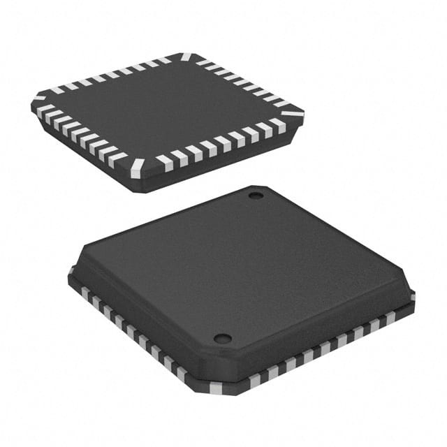
Texas Instruments VSP2582RHNR
- Part No.:
- VSP2582RHNR
- Manufacturer:
- Texas Instruments
- Category:
- Analog Front End (AFE)
- Package:
- 36-VFQFN
- Datasheet:
-
 VSP2582RHNR.pdf
- Description:
- IC AFE 1 CHAN 12BIT 36VQFN
- Quantity:
- Payment:

- Shipping:

Inventory:3,920
Please send an inquiry. Send us your inquiry, and we will respond immediately.
Product details
Overview
VSP2582RHNR from Texas Instruments is a 12-bit, 36-MHz CCD analog front-end IC for digital cameras, integrating correlated double sampling (CDS), programmable gain amplification (–9 dB to +35 dB), and input clamping with optical black (OB) level calibration. It processes CCD output signals in portable imaging systems requiring low power (85 mW at 3.0 V), stable black-level reference, and high SNR (78 dB input-referred at 0 dB CDS gain).
For engineers reviewing the VSP2582RHNR datasheet, VSP2582RHNR pinout, VSP2582RHNR application, or VSP2582RHNR equivalent, this device serves as a complete mixed-signal signal chain solution for CCD-based image capture-requiring attention to SHP/SHD timing alignment, OB loop capacitor selection (COB), serial register configuration (SDATA/SCLK/SLOAD), and thermal pad soldering per QFN-36 RHN package.
Technical Context
The VSP2582RHNR implements a two-stage gain architecture: analog CDS gain (–3 dB to +9 dB in 3-dB steps) followed by digital PGA (–6 dB to +26 dB in 0.03125-dB steps), enabling precise illumination-adaptive signal scaling without degrading OB clamp stability. Its CDS block uses dual-sampling clocking (SHP/SHD) with programmable polarity and sub-pixel sampling delay (0–2 ns).
Signal integrity is maintained via separate analog/digital supplies (VCC/VDD = 2.7–3.6 V), dedicated AGND/DGND planes, and on-chip reference generation (REFP = 1.5 V, REFN = 1.0 V). The OB calibration loop employs a 10-bit DAC driving COB to achieve 40.7 μs time constant (with 0.1 μF), supporting hot-pixel rejection and fast black-level recovery after gain changes.
Key Specifications
| Parameter | Value and Actual Design Meaning |
|---|---|
| Resolution | 12-bit ADC with no missing codes ensured across full scale |
| Conversion rate | 36 MHz maximum sampling - supports HD-resolution CCD readout at real-time frame rates |
| CDS gain range | –3 dB to +9 dB in 3-dB steps - primary analog amplification stage before digitization |
| Digital PGA range | –6 dB to +26 dB in 0.03125-dB steps - fine-grained adaptive gain control post-CDS |
| Input-referred SNR | 78 dB at 0 dB CDS gain - enables high-fidelity capture under low-light conditions |
| Power dissipation | 85 mW at 3.0 V/36 MHz; 1 mW in standby - suitable for battery-powered camera modules |
| Operating temperature | –25°C to +85°C - validated for consumer and industrial imaging environments |
Pinout & Package
Package: QFN-36 (RHN), 6 mm × 6 mm, exposed thermal pad (θJA = 81.0°C/W), RoHS-compliant.
| Pin/Terminal | Circuit Role | Design Meaning |
|---|---|---|
| B0–B11 | Digital output data (LSB to MSB) | 12-bit parallel CMOS outputs synchronized to ADCCK; B0 (pin 35), B11 (pin 10) |
| SHP / SHD | CCD sampling clocks | SHP samples reference level; SHD samples data level - defines CDS window timing |
| ADCCK | Digital output clock | Drives B0–B11 latching; output latency fixed at 6 clock cycles |
| CLPDM / CLPOB | Clamp control inputs | CLPDM activates input DC restoration during dummy pixels; CLPOB triggers OB calibration during OB pixels |
| CCDIN | Analog input | Single-ended CCD signal interface with 15 pF input capacitance and –0.3 V to 3.3 V voltage limit |
| VCC / VDD / AGND / DGND | Power and ground | Separate analog (pins 14,20,21,30) and digital (pin 11) supplies; multiple AGND pins (19,22,23,31) for noise isolation |
| SDATA / SCLK / SLOAD | Serial interface | 3-wire SPI-compatible bus (LSB-first) for configuring gain, clamp level, OB loop, and standby mode |
Key Features
| Feature | Design Value |
|---|---|
| Programmable black-level clamping | Configurable OB clamp level (64–312 LSB via 5-bit register) maintains consistent black reference across illumination changes |
| Hot-pixel rejection | Adjustable rejection threshold (via 5-bit register) prevents defective OB pixels from corrupting black-level calibration |
| Fast OB loop convergence | COB capacitor time constant configurable via DAC current scaling (x1/x2/x4/x8) to adapt to varying OB pixel count |
| Standby mode | Serial-command-activated state reducing power to 1 mW; resumes operation in ≤10 ms with zero output hold |
| Input signal clamping | Internal 1.5 V REFP reference used to restore DC bias during dummy pixel interval - eliminates baseline drift |
Applications
| Digital Still Camera | Security Surveillance Camera |
|---|---|
Use Scenario: Compact DSLR or mirrorless camera capturing still images under variable ambient light. IC Role / Device Role / Timing Role: Processes CCD output through CDS, PGA, and 12-bit ADC; synchronizes SHP/SHD to pixel clock; applies OB clamp during vertical blanking. Use Value: Delivers 78 dB SNR and stable black level across ISO settings, enabling clean RAW image data for downstream ISP processing. |
Use Scenario: Outdoor IP security camera operating 24/7 with auto-iris lens and low-light WDR capability. IC Role / Device Role / Timing Role: Digitizes interlaced CCD output; uses programmable digital gain to compensate for slow shutter speeds; leverages hot-pixel rejection to maintain calibration over sensor aging. Use Value: Ensures consistent image quality and black-level stability across temperature swings (–25°C to +85°C) and long-term deployment. |
| Medical Endoscope Imaging | Industrial Machine Vision |
Use Scenario: High-resolution endoscopic system requiring minimal power and EMI-sensitive analog signal integrity. IC Role / Device Role / Timing Role: Front-end signal conditioner for small-format CCD; isolates analog/digital domains via separate VCC/VDD and AGND/DGND routing; uses internal REFP/REFN references. Use Value: Achieves diagnostic-grade image fidelity with 12-bit linearity (±2 LSB INL) and no missing codes - critical for tissue contrast analysis. |
Use Scenario: Automated optical inspection (AOI) system scanning PCBs or semiconductor wafers using line-scan CCDs. IC Role / Device Role / Timing Role: Provides precise pixel-level timing control (SHP/SHD/ADCCK alignment within ±3 ns); supports high-speed 36-MHz digitization of fast-moving linear arrays. Use Value: Enables sub-pixel measurement accuracy and repeatable grayscale linearity across production batches. |
Equivalent & Alternatives
The following parts are listed as comparable options for similar CCD analog front-end applications.
| Alternative Part | Technical Difference | Application Difference | Selection Advice |
|---|---|---|---|
| TAS5381AIPAG | 14-bit, 40-MHz ADC; integrated LDOs; no OB loop or CLPDM/CLPOB support | Designed for audio-class sigma-delta conversion, not CCD-specific timing or clamping | Not suitable for CCD systems requiring OB calibration or dummy-pixel clamping |
| AD9945KSTZ | 12-bit, 30-MHz; includes on-chip PLL and sync generator; CDS gain limited to –6 dB to +24 dB | Targets broadcast video CCDs with embedded timing gen; lacks hot-pixel rejection and fast OB recovery | Acceptable for fixed-gain broadcast cameras but inferior for portable/low-power or adaptive-illumination use cases |
Compared with VSP2582RHNR, AD9945KSTZ offers integrated timing generation but lower CDS flexibility and no hot-pixel mitigation, while TAS5381AIPAG is functionally misaligned for CCD signal conditioning - making VSP2582RHNR uniquely suited for portable, OB-critical, and thermally constrained CCD imaging designs.
Availability
VSP2582RHNR is available at Aetrix Electronics and suitable for digital camera modules, security surveillance systems, and medical endoscopy equipment requiring stable component supply, long-lifecycle support, and QFN-36 thermal performance.
Supply support for VSP2582RHNR includes scheduled delivery planning, volume procurement assistance, BOM continuity management, traceable sourcing, and lifecycle availability coordination for OEM customers, industrial embedded developers, connected-device designers, and electronics production programs.
Manufacturer
Texas Instruments is a global semiconductor company specializing in analog, embedded processing, and digital signal technologies, with leadership in precision signal chain solutions.
The VSP2582RHNR belongs to TI's CCD analog front-end product line, engineered specifically for high-fidelity, low-power digitization of charge-coupled device outputs in portable and industrial imaging systems.
FAQ
What is the function of the CLPOB and CLPDM pins on the VSP2582RHNR?
The CLPOB pin activates the optical black (OB) level calibration loop during OB pixel readout, enabling automatic offset compensation. The CLPDM pin enables input signal clamping to REFP (1.5 V) during dummy pixel intervals to restore DC bias. Both must be asserted separately - never simultaneously - and their active polarity is programmable via the Clk-Pol-ctrl register. This dual-clamp architecture ensures stable black-level reference and accurate pixel-level digitization in the VSP2582RHNR.
Does the VSP2582RHNR support true 12-bit performance across its full operating range?
Yes, the VSP2582RHNR guarantees no missing codes and specifies ±2 LSB integral nonlinearity (INL) and ±0.5 LSB differential nonlinearity (DNL) at 0 dB CDS gain and 0 dB DPGA gain. Measured SNR of 78 dB input-referred confirms effective resolution exceeds 12 bits under optimal conditions. Performance remains validated across the full –25°C to +85°C temperature range and 2.7–3.6 V supply, confirming true 12-bit fidelity in production use of the VSP2582RHNR.
How does the VSP2582RHNR handle black-level stability when digital gain is adjusted?
The VSP2582RHNR maintains black-level stability during digital gain changes because the optical black (OB) clamp loop operates upstream of the digital PGA stage. OB calibration occurs in the analog domain using CDS output, and the resulting clamp level is applied before digital gain scaling. This architecture ensures that black-level reference remains invariant regardless of DPGA setting - a key design feature confirmed in the VSP2582RHNR functional description and timing diagrams.
What thermal considerations apply to the VSP2582RHNR's QFN-36 RHN package?
The VSP2582RHNR in QFN-36 RHN package requires soldering of the exposed thermal pad to a solid copper plane for effective heat dissipation. With θJA = 81.0°C/W, junction temperature rise is ~6.9°C at 85 mW (3.0 V/36 MHz). TI recommends ≥4 thermal vias under the pad connected to inner-layer ground planes. The RHN variant's higher θJA versus RHH (31.7°C/W) reflects its tray packaging - thermal design must prioritize pad connectivity and airflow in compact camera modules using the VSP2582RHNR.
Can the VSP2582RHNR operate with a single 3.0 V supply, and how are analog and digital domains isolated?
Yes, the VSP2582RHNR operates from a single 3.0 V nominal supply, but it mandates separate analog (VCC) and digital (VDD) rail connections - both rated 2.7–3.6 V - with independent AGND and DGND grounds. Internal regulators and layout separation ensure analog signal integrity. Decoupling requires 0.1 μF (BYP/REFP/REFN) and 1000 pF (BYPP) capacitors placed near respective pins. This dual-supply, multi-ground architecture is essential to achieve 78 dB SNR and is explicitly required in all VSP2582RHNR reference designs.
VSP2582RHNR Specifications
- Product attributes
- Attribute value
- Manufacturer:
- Texas Instruments
- package:
- 36-VFQFN
- Series:
- -
- Packaging:
- Tape & Reel (TR)
- Product Status:
- Obsolete
- Number of Bits:
- 12
- Number of Channels:
- 1
- Power (Watts):
- 85 mW
- Voltage - Supply, Analog:
- 2.7V ~ 3.6V
- Voltage - Supply, Digital:
- 2.7V ~ 3.6V
- Mounting Type:
- Surface Mount
- Grade:
- -
- Qualification:
- -
VSP2582RHNR FAQ
1.How can I place an order for VSP2582RHNR through Aetrix?
Please submit a Request for Quotation (RFQ) for VSP2582RHNR on Aetrix. Our sales agent will provide a competitive quotation and guide you through the order confirmation once you accept the terms.
2.Are the price and stock information for VSP2582RHNR reliable?
The price and inventory of VSP2582RHNR are updated periodically and may fluctuate due to market conditions. Stock and pricing data are typically refreshed every 24 hours. Quotation validity for VSP2582RHNR is usually 5 days.
3.What payment methods are accepted for VSP2582RHNR?
We accept Wire Transfer, PayPal, Credit Card, Western Union, MoneyGram, and Escrow for VSP2582RHNR transactions.
Note: Certain payment methods may incur a processing fee.
4.How is shipping managed for VSP2582RHNR?
VSP2582RHNR orders can be shipped via leading logistics carriers, including DHL, UPS, FedEx, TNT, or Registered Mail.
Once your VSP2582RHNR order is processed, you will receive an email with the shipment details and tracking number.
Note: Tracking information may take up to 24 hours to appear. Express delivery typically takes 3–5 business days.
5.How can I obtain technical support or documentation for VSP2582RHNR?
For technical support, including VSP2582RHNR datasheets, pinout diagrams, or application guidance, please contact our engineering support team. They can provide detailed documentation and assistance for your VSP2582RHNR requirements.
6.How does Aetrix verify that VSP2582RHNR is sourced from the original manufacturer or authorized distributors?
All VSP2582RHNR products on Aetrix are procured from qualified distributors and authorized channels. Our dedicated quality assurance team conducts strict verification, including traceability checks and, if necessary, third-party testing. This ensures that VSP2582RHNR meets industry standards.
7.What is the process for return or replacement of VSP2582RHNR?
All VSP2582RHNR units undergo pre-shipment inspection (PSI). If there is an issue with VSP2582RHNR, returns or replacements are accepted under the following conditions:
1.Quantity discrepancies, incorrect items, or visible external defects (such as breakage or corrosion), acknowledged by Aetrix.
2.The issue is reported within 90 days of delivery.
3.The VSP2582RHNR part is unused and in its original packaging.
Return procedure for VSP2582RHNR:
1.Submit a request within 90 days.
2.Obtain a Return Material Authorization (RMA) from Aetrix.
VSP2582RHNR Tags
-
MCP3911A0-E/SS
Microchip Technology
-
ADS131A04IPBSR
Texas Instruments
-
ADS1292RIPBSR
Texas Instruments
-
ADS1292IRSMT
Texas Instruments

-
LMP90097MHE/NOPB
Texas Instruments
-
AD5940BCBZ-RL
Analog Devices Inc.
-
AD5940BCBZ-RL7
Analog Devices Inc.
-
AD5941BCPZ-RL7
Analog Devices Inc.
-
AD5941BCPZ
Analog Devices Inc.
-
ADS131E08IPAGR
Texas Instruments

-
LMP90100MH/NOPB
Texas Instruments
-
LMP90100MHE/NOPB
Texas Instruments
Tech Hub

A practical engineering guide to 3.3V and 5V logic compatibility, input thresholds, resistor dividers, translator ICs, MOSFET level shifting, I2C pull-ups, timing limits and power-sequencing risks.

The 74HC595 uses push-pull logic outputs, while the TPIC6B595 uses 50 V open-drain DMOS sinks for higher-power loads. This guide compares timing, current limits, 3.3 V interfacing, load wiring, thermal…

The 74HC595 converts serial data into eight stable parallel outputs. This guide covers pin functions, shift and storage timing, OE and MR behavior, drive-current limits, cascading, voltage compatibilit…

A technical comparison of level-sensitive latches and edge-triggered flip-flops, covering timing windows, setup and hold limits, master–slave operation, time borrowing, race-through, HDL inference and…

A D latch stores one bit while Enable controls when data can pass. This reference covers gate-level operation, truth tables, transparency, setup and hold timing, LE versus OE, common ICs and practical …

An SR latch stores one bit through cross-coupled feedback. This engineering reference covers NOR and NAND implementations, truth tables, forbidden-state recovery, gated operation, switch debouncing, fa…

Latch circuits retain one bit through feedback. This technical reference covers SR and D latches, truth tables, transparency, timing limits, latch-versus-flip-flop behavior, applications and common log…

An engineering guide to LED driver operation, constant-current and constant-voltage outputs, linear and switching topologies, dimming, IC selection, calculations, replacement compatibility, and fault c…

Operational amplifier guide covering op amp basics, feedback, ideal vs real op amps, common configurations, buffer circuits, offset, bias current, gain-bandwidth, slew rate, rail-to-rail limits and sel…

Jumper cables guide covering safe connection order, red and black clamp placement, final ground connection, cable gauge, length, clamp quality, copper vs CCA cables, jump starter comparison and battery…


