
 My Inquiry
 My Account


Infineon Technologies W134MH
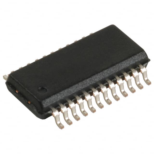
- Part No.:
- W134MH
- Manufacturer:
- Infineon Technologies
- Package:
- 24-SSOP (0.154", 3.90mm Width)
- Datasheet:
-
 W134MH.pdf
- Description:
- IC CLOCK/FREQ GEN 24QSOP
- Quantity:
- Payment:

- Shipping:

Inventory:1,878
Please send an inquiry. Send us your inquiry, and we will respond immediately.
Product details
Overview
W134MH from Cypress Semiconductor is a Direct Rambus™ Clock Generator IC that provides differential RSL clock outputs for Rambus memory subsystems, supporting up to 800-MHz data transfer rates. It implements a PLL-based clock synthesis with distributed delay-locked loop (DDLL) phase alignment, accepts REFCLK up to 100 MHz, operates at 3.3 V, and features STOPB and PWRDNB control inputs for dynamic clock gating and power-down in mobile platforms.
For engineers reviewing the W134MH datasheet, W134MH pinout, W134MH application, or W134MH equivalent, this device is selected for Intel architecture platforms requiring precise phase-synchronized Rambus channel clocks, low-jitter timing alignment between Pclk/M and Synclk/N domains, and configurable PLL multiplication ratios (4×–16×) via MULT0/MULT1 pins.
Technical Context
The W134MH integrates a PLL with programmable feedback (A) and prescaler (B) dividers to generate Busclk from REFCLK, enabling gear-ratio-based synchronization between processor (Pclk) and Rambus (Synclk) domains. Its phase detector compares PCLKM and SYNCLKN signals-both derived from M/N-divided clocks-to drive a phase aligner that adjusts Busclk phase until rising edges align within ±50 ps.
It supports four operating modes (Normal, Bypass, Output Test, Test) via S0/S1 pins, includes dedicated voltage references (VDDIR for REFCLK, VDDIPD for phase detector), and delivers Rambus Signaling Level (RSL) complementary outputs (CLK/CLKB) with 40/60% worst-case duty cycle and Hi-Z capability during StopB or PWRDNB assertion.
Key Specifications
| Parameter | Value and Actual Design Meaning |
|---|---|
| Supply Voltage | 3.3 V ±0.165 V - powers core logic and RSL output buffers; requires stable low-noise supply |
| REFCLK Max Frequency | 100 MHz - sets upper limit for input reference clock; determines achievable Busclk via A/B ratio |
| Output Type | Rambus Signaling Level (RSL) - differential swing compatible with RDRAM termination and channel impedance |
| Duty Cycle | 40/60% worst case - ensures timing margin for Rambus channel setup/hold requirements |
| Phase Alignment Accuracy | ±50 ps settled phase error - guarantees sub-cycle alignment between Pclk/M and Synclk/N domains |
| Operating Temperature | 0°C to +70°C - validated for commercial-grade desktop and embedded Intel platform operation |
| Power-down Recovery | 3 ms max tPOWERUP - defines minimum latency before glitch-free CLK/CLKB output after PWRDNB deassertion |
Pinout & Package
W134MH is housed in a 24-pin QSOP (150-mil SSOP) package with exposed pad thermal design, pin-compatible with W134M/W134S variants and optimized for high-density Rambus channel routing.
| Pin/Terminal | Circuit Role | Design Meaning |
|---|---|---|
| REFCLK (Pin 2) | Reference Clock Input | Primary frequency source for PLL; typically driven by Cypress W133 or system synthesizer at half FSB rate |
| PCLKM (Pin 6), SYNCLKN (Pin 7) | Phase Detector Inputs | Accept M/N-divided clocks from Gear Ratio Logic; used to lock phase of Busclk to Pclk domain |
| STOPB (Pin 11), PWRDNB (Pin 12) | Active-Low Control Inputs | STOPB disables CLK/CLKB drivers (Hi-Z); PWRDNB powers down PLL and forces outputs to GND |
| MULT0/MULT1 (Pins 14–15) | PLL Multiplier Select | Set A/B divider values (e.g., 8/1 → 8×, 6/1 → 6×) to configure Busclk = REFCLK × A/B |
| CLK/CLKB (Pins 18, 20) | Differential RSL Outputs | Terminated complementary clocks for Rambus Channel; require 28 Ω series resistors per leg |
| S0/S1 (Pins 23–24) | Mode Control Inputs | Select Normal, Bypass (PLLclk direct), Output Test (Hi-Z), or Test (REFCLK pass-through) |
Key Features
| Feature | Design Value |
|---|---|
| Distributed DDLL Phase Alignment | Enables zero-latency data exchange between Pclk and Synclk domains by dynamically adjusting Busclk phase to match Pclk/M vs. Synclk/N edge alignment |
| Configurable PLL Multiplication | Four discrete A/B ratios (4×–16×) selectable via MULT0/MULT1, supporting 267–400 MHz Busclk from 33–67 MHz REFCLK |
| Multi-mode Operation | Hardware-selectable Bypass (full-speed PLL output), Output Test (Hi-Z), and Test (REFCLK pass-through) modes simplify board bring-up and validation |
| Mobile Power Management | Independent STOPB and PWRDNB inputs allow clock gating (low-power idle) or full shutdown (deep sleep), reducing system standby current |
| Dedicated Voltage References | VDDIR (Pin 1) and VDDIPD (Pin 10) isolate REFCLK and phase detector thresholds from core supply noise, improving jitter immunity |
Applications
| Intel Pentium III Desktop Platforms | Rambus RDRAM Memory Subsystems |
|---|---|
|
Use Scenario: Mainboard implementation with 133 MHz front-side bus and 400 MHz Rambus channel. IC Role / Device Role / Timing Role: Generates synchronized Busclk and enables Gear Ratio Logic to align Pclk/M and Synclk/N at 33 MHz for zero-latency domain crossing. Use Value: Eliminates inter-domain synchronization latency, enabling full bandwidth utilization of RDRAM without pipeline stalls. |
Use Scenario: Dual-channel RDRAM module interface with matched trace routing and on-die termination. IC Role / Device Role / Timing Role: Provides low-skew, RSL-compliant CLK/CLKB pair with 40/60% duty cycle and ±50 ps phase stability across temperature. Use Value: Ensures signal integrity over 12-inch channel lengths while meeting Rambus JEDEC timing windows for read/write strobes. |
| Mobile Intel Architecture Notebooks | Legacy Server Memory Controllers |
|
Use Scenario: Battery-powered laptop with dynamic CPU frequency scaling and RDRAM power gating. IC Role / Device Role / Timing Role: Uses PWRDNB to disable PLL and STOPB to gate outputs during C3/C4 sleep states, cutting clock-related leakage. Use Value: Reduces active/idle power consumption by >90% versus always-on clock generators, extending battery life. |
Use Scenario: Dual-processor server motherboard with redundant Rambus channels and ECC support. IC Role / Device Role / Timing Role: Delivers fail-safe clock enable/disable sequencing via STOPB and PWRDNB, coordinated with memory controller reset states. Use Value: Prevents metastability during hot-plug or warm-reset events by ensuring CLK/CLKB enter known Hi-Z or GND states. |
Equivalent & Alternatives
Cypress W134MH has two functionally aligned alternatives with documented compatibility in Intel platform reference designs.
| Alternative Part | Technical Difference | Application Difference | Selection Advice |
|---|---|---|---|
| Cypress W134S | Same pinout and functionality; differs only in PLL A/B divider mapping (e.g., MULT0=0,MULT1=0 → 4× vs. W134M's 9×) | Optimized for lower REFCLK frequencies (e.g., 50 MHz) targeting 300–400 MHz Busclk with tighter gear ratios | Select W134S when REFCLK ≤ 50 MHz and target Busclk requires integer M/N ratios like 4:3 or 8:6 |
| Cypress W134M | Identical package and pinout; differs in default PLL multiplier set (e.g., 9×, 6×, 8×, 16×) versus W134S's 4×, 6×, 8×, 16× | Better suited for higher REFCLK (67 MHz) and 267–400 MHz Busclk with 2:2 or 4:2 gear ratios | Choose W134M when REFCLK ≥ 67 MHz and system uses Pclk=133 MHz with M=4,N=2 configuration |
Compared with W134S and W134M, W134MH shares identical packaging, pinout, and mode logic but is distinguished by its specific A/B divider table and qualification for mixed-voltage Intel chipset environments-making it the preferred choice where REFCLK sourcing and gear-ratio constraints demand exact multiplier matching.
Availability
W134MH is available at Aetrix Electronics and suitable for Intel Pentium III desktop platforms, Rambus RDRAM memory subsystems, and mobile Intel architecture notebooks requiring stable component supply and long-term lifecycle support.
Supply support for W134MH includes scheduled delivery planning, volume procurement assistance, BOM continuity management, traceable sourcing, and lifecycle availability coordination for OEM customers, industrial embedded developers, connected-device designers, and electronics production programs.
Manufacturer
Cypress Semiconductor (now part of Infineon Technologies) is a fabless semiconductor company specializing in timing, memory interface, and programmable logic solutions for computing and communications infrastructure.
The W134MH belongs to Cypress's Direct Rambus Clock Generator product line, engineered specifically to meet Intel's DDLL architecture requirements for phase-aligned, low-jitter clock distribution in RDRAM-based platforms.
FAQ
What is the function of VDDIPD and how must it be connected?
VDDIPD (Pin 10) serves as the voltage reference for the phase detector inputs (PCLKM, SYNCLKN) and STOPB threshold. It must be connected to the same supply rail that powers the memory controller's output drivers-typically 2.5 V or 3.3 V-not the core VDD. Incorrect connection causes phase detection failure or erratic STOPB response due to mismatched input thresholds.
Can W134MH operate without Gear Ratio Logic?
Yes. When Gear Ratio Logic is absent, PCLKM and SYNCLKN must be tied to GND per datasheet guidance. The device then operates in free-running PLL mode using only REFCLK and MULT0/MULT1 settings. Output frequency equals REFCLK × A/B, but phase synchronization to the processor clock is disabled-suitable only for non-synchronous Rambus implementations.
What happens to CLK/CLKB during PWRDNB assertion?
When PWRDNB is driven LOW, the internal PLL shuts down, all logic blocks are powered off, and CLK/CLKB outputs are actively driven to GND (not Hi-Z). This differs from STOPB, which places outputs in high-impedance state. PWRDNB ensures zero static current draw and eliminates any residual clock feedthrough during deep sleep states.
How does the Bypass mode differ from Normal mode in timing behavior?
In Bypass mode (S0=1,S1=0), the full-speed PLL output (PLLclk) appears directly at CLK/CLKB, skipping the phase aligner. This removes DDLL-induced latency but sacrifices phase alignment between Pclk and Synclk domains. Normal mode routes PLLclk through the phase aligner, adding ~2 ns propagation delay but guaranteeing ±50 ps edge alignment critical for zero-latency data transfers.
W134MH Specifications
- Product attributes
- Attribute value
- Manufacturer:
- Infineon Technologies
- Series:
- -
- Package/Case:
- 24-SSOP (0.154", 3.90mm Width)
- Packaging:
- Tube
- Product Status:
- Obsolete
- Programmable:
- Not Verified
- Type:
- Clock/Frequency Generator
- PLL:
- Yes
- Input:
- Clock
- Output:
- RSL
- Number of Circuits:
- 1
- Ratio - Input:Output:
- 1:1
- Differential - Input:Output:
- No/Yes
- Frequency - Max:
- 400MHz
- Divider/Multiplier:
- Yes/Yes
- Voltage - Supply:
- 3.135V ~ 3.465V
- Operating Temperature:
- 0°C ~ 70°C
- Mounting Type:
- Surface Mount
- Grade:
- -
- Qualification:
- -
- Supplier Device Package:
- 24-QSOP
W134MH FAQ
1.How can I place an order for W134MH through Aetrix?
Please submit a Request for Quotation (RFQ) for W134MH on Aetrix. Our sales agent will provide a competitive quotation and guide you through the order confirmation once you accept the terms.
2.Are the price and stock information for W134MH reliable?
The price and inventory of W134MH are updated periodically and may fluctuate due to market conditions. Stock and pricing data are typically refreshed every 24 hours. Quotation validity for W134MH is usually 5 days.
3.What payment methods are accepted for W134MH?
We accept Wire Transfer, PayPal, Credit Card, Western Union, MoneyGram, and Escrow for W134MH transactions.
Note: Certain payment methods may incur a processing fee.
4.How is shipping managed for W134MH?
W134MH orders can be shipped via leading logistics carriers, including DHL, UPS, FedEx, TNT, or Registered Mail.
Once your W134MH order is processed, you will receive an email with the shipment details and tracking number.
Note: Tracking information may take up to 24 hours to appear. Express delivery typically takes 3–5 business days.
5.How can I obtain technical support or documentation for W134MH?
For technical support, including W134MH datasheets, pinout diagrams, or application guidance, please contact our engineering support team. They can provide detailed documentation and assistance for your W134MH requirements.
6.How does Aetrix verify that W134MH is sourced from the original manufacturer or authorized distributors?
All W134MH products on Aetrix are procured from qualified distributors and authorized channels. Our dedicated quality assurance team conducts strict verification, including traceability checks and, if necessary, third-party testing. This ensures that W134MH meets industry standards.
7.What is the process for return or replacement of W134MH?
All W134MH units undergo pre-shipment inspection (PSI). If there is an issue with W134MH, returns or replacements are accepted under the following conditions:
1.Quantity discrepancies, incorrect items, or visible external defects (such as breakage or corrosion), acknowledged by Aetrix.
2.The issue is reported within 90 days of delivery.
3.The W134MH part is unused and in its original packaging.
Return procedure for W134MH:
1.Submit a request within 90 days.
2.Obtain a Return Material Authorization (RMA) from Aetrix.
W134MH Tags

-
CD74HCT4046AM96
Texas Instruments

-
MC14046BDWR2G
onsemi

-
501MILFT
Renesas Electronics Corporation
-
CD74HC7046AM
Texas Instruments

-
CDCVF2505PWR
Texas Instruments

-
RC19004A100GNL#KB0
Renesas Electronics Corporation

-
SI5351A-B-GTR
Skyworks Solutions Inc.

-
CY2305SXI-1T
Infineon Technologies
-
570BILFT
Renesas Electronics Corporation

-
CDCE913PWR
Texas Instruments
-
CY2305SXI-1HT
Infineon Technologies

-
DS1086LU+T
Analog Devices Inc./Maxim Integrated
Tech Hub

An engineering guide to LED driver operation, constant-current and constant-voltage outputs, linear and switching topologies, dimming, IC selection, calculations, replacement compatibility, and fault c…

Operational amplifier guide covering op amp basics, feedback, ideal vs real op amps, common configurations, buffer circuits, offset, bias current, gain-bandwidth, slew rate, rail-to-rail limits and sel…

Jumper cables guide covering safe connection order, red and black clamp placement, final ground connection, cable gauge, length, clamp quality, copper vs CCA cables, jump starter comparison and battery…

LDO regulator guide covering low dropout voltage, power dissipation, thermal design, PSRR, output noise, capacitor stability, adjustable LDO circuits, LDO vs buck converter and datasheet selection chec…

Conditional Access Module guide covering CAM meaning, CI/CI+ interface, smart card authorization, DVB security workflow, TV and set-top box compatibility, internal electronics, ESD protection, connecto…

Guide to electronic component obsolescence covering EOL risk, PCN/PDN notices, last-time buy planning, replacement options, form-fit-function validation, counterfeit risk and BOM lifecycle management.

18650 battery guide covering lithium-ion cell basics, 3.6V/3.7V voltage, 4.2V charging, mAh and Wh capacity, protected cells, chargers, BMS, series-parallel packs, holders, welding and sourcing checks.…

Hall effect sensor guide covering working principle, linear and digital sensors, Arduino circuits, current sensing, speed detection, automotive applications, A3144 examples, signal filtering and datash…

Product Change Notification guide for electronic components, covering PCN meaning, PCN vs PDN/EOL, common change types, risk levels, form-fit-function review, engineering validation, BOM control, LTB/L…

A practical guide to blend door actuators, covering HVAC function, symptoms, location, AC and heater issues, reset and calibration, replacement cost, electrical diagnosis, compatibility checks, and rep…


